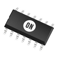
MC33274AD ON Semiconductor, MC33274AD Datasheet - Page 2

MC33274AD
Manufacturer Part Number
MC33274AD
Description
Op Amps 3-36V Quad Low Noise
Manufacturer
ON Semiconductor
Datasheet
1.MC33274APG.pdf
(16 pages)
Specifications of MC33274AD
Number Of Channels
4
Voltage Gain Db
100 dB
Common Mode Rejection Ratio (min)
80 dB
Input Voltage Range (max)
Positive Rail - 1.8 V
Input Voltage Range (min)
Negative Rail
Input Offset Voltage
2 mV
Operating Supply Voltage
36 V
Supply Current
8.6 mA
Maximum Operating Temperature
+ 85 C
Mounting Style
SMD/SMT
Package / Case
SOIC-14
Maximum Dual Supply Voltage
+/- 18 V
Minimum Operating Temperature
- 40 C
Lead Free Status / Rohs Status
No
Available stocks
Company
Part Number
Manufacturer
Quantity
Price
Part Number:
MC33274AD
Manufacturer:
ON/安森美
Quantity:
20 000
Company:
Part Number:
MC33274ADG
Manufacturer:
ON Semiconductor
Quantity:
5
Part Number:
MC33274ADG
Manufacturer:
ON/安森美
Quantity:
20 000
Company:
Part Number:
MC33274ADR
Manufacturer:
XG
Quantity:
13 410
Company:
Part Number:
MC33274ADR2G
Manufacturer:
ON Semiconductor
Quantity:
2 100
Part Number:
MC33274ADR2G
Manufacturer:
ON/安森美
Quantity:
20 000
Part Number:
MC33274ADT
Manufacturer:
ON/安森美
Quantity:
20 000
Company:
Part Number:
MC33274ADTBR2G
Manufacturer:
ON Semiconductor
Quantity:
1 400
Part Number:
MC33274ADTBR2G
Manufacturer:
ON/安森美
Quantity:
20 000
Stresses exceeding Maximum Ratings may damage the device. Maximum Ratings are stress ratings only. Functional operation above the
Recommended Operating Conditions is not implied. Extended exposure to stresses above the Recommended Operating Conditions may affect
device reliability.
1. Either or both input voltages should not exceed V
2. Power dissipation must be considered to ensure maximum junction temperature (T
MAXIMUM RATINGS
Supply Voltage
Input Differential Voltage Range
Input Voltage Range
Output Short Circuit Duration (Note 2)
Maximum Junction Temperature
Storage Temperature
ESD Protection at Any Pin
Maximum Power Dissipation
Operating Temperature Range
Inputs 1
Output 1
V
EE
CASE 626/751
1
2
3
4
Rating
(Top View)
-
+
DUAL
+
-
8
7
6
5
Output 2
V
NCV33272A, NCV33274A
CC
Inputs 2
MC33272A, MC33274A
− Human Body Model
CC
− Machine Model
or V
PIN CONNECTIONS
http://onsemi.com
EE
.
2
Inputs 1
Inputs 2
Output 1
Output 2
V
V
CC
Symbol
CC
V
V
CASE 646/751A/948G
T
V
t
P
T
T
SC
to V
IDR
esd
stg
1
2
3
4
5
6
7
J
IR
D
A
J
) is not exceeded (see Figure 2).
EE
-
+
+
-
(Top View)
QUAD
2
1
3
4
+
-
-
+
14
13
12
11
10
−60 to +150
−40 to +125
9
8
−40 to +85
Indefinite
Output 4
V
Output 3
Note 1
Note 1
Note 2
Value
+150
2000
EE
+36
200
Inputs 4
Inputs 3
Unit
mW
sec
°C
°C
°C
V
V
V
V


