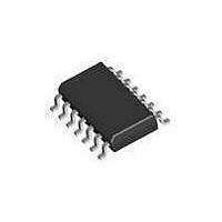
74LVC02APW NXP Semiconductors, 74LVC02APW Datasheet - Page 9

74LVC02APW
Manufacturer Part Number
74LVC02APW
Description
Gates (AND / NAND / OR / NOR) 3.3V QUAD 2-INPUT NOR GATE
Manufacturer
NXP Semiconductors
Datasheet
1.74LVC02ABQ115.pdf
(15 pages)
Specifications of 74LVC02APW
Product
NOR
Logic Family
LVC
Number Of Gates
4
Number Of Lines (input / Output)
2 / 1
High Level Output Current
- 24 mA
Low Level Output Current
24 mA
Propagation Delay Time
14 ns
Supply Voltage (max)
3.6 V
Supply Voltage (min)
1.2 V
Maximum Operating Temperature
+ 125 C
Mounting Style
SMD/SMT
Package / Case
TSSOP-14
Minimum Operating Temperature
- 40 C
Lead Free Status / Rohs Status
Details
Other names
74LVC02APW,112
Available stocks
Company
Part Number
Manufacturer
Quantity
Price
Company:
Part Number:
74LVC02APW
Manufacturer:
TI
Quantity:
1 155
Part Number:
74LVC02APW
Manufacturer:
PHILIPS/飞利浦
Quantity:
20 000
Philips Semiconductors
AC WAVEFORMS
2004 Mar 12
handbook, full pagewidth
Quad 2-input NOR gate
V
V
V
Note
1. The circuit performs better when RL = 1000 .
Definitions for test circuit:
R
C
R
1.2 V
2.7 V
3.0 V to 3.6 V
M
M
OL
L
L
T
= Load resistor.
= Load capacitance including jig and probe capacitance.
= Termination resistance should be equal to the output impedance Z
= 1.5 V at V
= 0.5
and V
V
OH
V
CC
CC
are typical output voltage drop that occur with the output load.
CC
at V
CC
2.7 V;
< 2.7 V;
V
2.7 V
2.7 V
CC
V
I
GENERATOR
handbook, halfpage
Fig.6 The input nA, nB to output nY propagation delays.
PULSE
50 pF
50 pF
50 pF
nA, nB input
nY output
C
L
Fig.7 Load circuitry for switching times.
V I
500
500
500
R
R T
L
V M
t PHL
(1)
D.U.T.
V CC
open
open
open
V M
t
PLH
o
of the pulse generator.
9
/t
V O
PHL
SWITCH S1
GND
GND
GND
t
PZH
50 pF
C L
t PLH
/t
PHZ
500
500
R L
R L
MNA213
2
2
2
t
PZL
S1
V
V
V
/t
CC
CC
CC
PLZ
MNA368
2
open
GND
V CC
Product specification
74LVC02A


