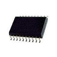
74LVT244ADB-T NXP Semiconductors, 74LVT244ADB-T Datasheet - Page 4

74LVT244ADB-T
Manufacturer Part Number
74LVT244ADB-T
Description
Buffers & Line Drivers 3.3V OCTAL 3-S DRVER
Manufacturer
NXP Semiconductors
Datasheet
1.74LVTH244AD118.pdf
(15 pages)
Specifications of 74LVT244ADB-T
Logic Family
LVT
Logic Type
BiCMOS
Number Of Channels Per Chip
8
Polarity
Non-Inverting
Supply Voltage (max)
3.6 V
Supply Voltage (min)
2.7 V
Maximum Operating Temperature
+ 85 C
Mounting Style
SMD/SMT
Package / Case
SOT-339-20
High Level Output Current
- 32 mA
Low Level Output Current
64 mA
Minimum Operating Temperature
- 40 C
Number Of Lines (input / Output)
8 / 8
Output Type
3-State
Propagation Delay Time
2.6 ns at 3.3 V
Lead Free Status / Rohs Status
Details
Other names
74LVT244ADB,118
NXP Semiconductors
6. Functional description
Table 3.
[1]
7. Limiting values
Table 4.
In accordance with the Absolute Maximum Rating System (IEC 60134). Voltages are referenced to GND (ground = 0 V).
[1]
[2]
[3]
8. Recommended operating conditions
Table 5.
74LVT_LVTH244A_4
Product data sheet
Control
nOE
L
H
Symbol
V
V
V
I
I
I
T
T
P
Symbol
V
V
I
IK
OK
O
OH
stg
j
CC
I
O
tot
CC
I
H = HIGH voltage level; L = LOW voltage level; X = don’t care; Z = high-impedance OFF-state.
The input and output negative voltage ratings may be exceeded if the input and output clamp current ratings are observed.
The performance capability of a high-performance integrated circuit in conjunction with its thermal environment can create junction
temperatures which are detrimental to reliability.
For SO20 packages: above 70 C derate linearly with 8 mW/K.
For SSOP20 and TSSOP20 packages: above 60 C derate linearly with 5.5 mW/K.
For DHVQFN20 packages: above 60 C derate linearly with 4.5 mW/K.
Parameter
supply voltage
input voltage
HIGH-level output current
Function table
Limiting values
Operating conditions
Parameter
supply voltage
input voltage
output voltage
input clamping current
output clamping current
output current
storage temperature
junction temperature
total power dissipation
6.1 Function table
[1]
Input
nAn
L
H
X
Conditions
Rev. 04 — 3 September 2008
Conditions
output in OFF-state or
HIGH-state
V
V
output in LOW-state
output in HIGH-state
T
amb
I
O
< 0 V
< 0 V
= 40 to +85 C
74LVT244A; 74LVTH244A
3.3 V octal buffer/line driver; 3-state
Output
nYn
L
H
Z
[1]
[1]
[2]
[3]
Min
-
-
-
-
-
0.5
0.5
0.5
65
Min
2.7
0
-
Typ
-
-
-
Max
+4.6
+7.0
+7.0
128
+150
150
500
50
50
64
© NXP B.V. 2008. All rights reserved.
Max
3.6
5.5
32
Unit
V
V
V
mA
mA
mA
mA
mW
C
C
Unit
V
V
mA
4 of 15


