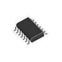
74ABT00D NXP Semiconductors, 74ABT00D Datasheet - Page 4

74ABT00D
Manufacturer Part Number
74ABT00D
Description
Gates (AND / NAND / OR / NOR) QUAD 2-IN NAND GATE
Manufacturer
NXP Semiconductors
Datasheet
1.74ABT00D112.pdf
(10 pages)
Specifications of 74ABT00D
Product
NAND
Logic Family
74ABT
Number Of Gates
Quad
Number Of Lines (input / Output)
2 / 4
High Level Output Current
- 15 mA
Low Level Output Current
20 mA
Propagation Delay Time
4.1 ns
Supply Voltage (max)
5.5 V
Supply Voltage (min)
4.5 V
Maximum Operating Temperature
+ 85 C
Mounting Style
SMD/SMT
Package / Case
SOT-108
Minimum Operating Temperature
- 40 C
Lead Free Status / Rohs Status
Details
Other names
74ABT00D,112
Available stocks
Company
Part Number
Manufacturer
Quantity
Price
Company:
Part Number:
74ABT00D
Manufacturer:
NXP Semiconductors
Quantity:
1 782
Part Number:
74ABT00DB
Manufacturer:
PHILIPS/飞利浦
Quantity:
20 000
1. Skew is defined as the absolute value of the difference between the actual propagation delay for any two separate outputs of the same
Philips Semiconductors
AC CHARACTERISTICS
GND = 0V; t
NOTE:
AC WAVEFORMS
V
TEST CIRCUIT AND WAVEFORMS
1995 Sep 18
M
SYMBOL
Quad 2-input NAND gate
device. The specification applies to any outputs switching in the the same direction, either HIGH-to-LOW (t
parameter guaranteed by design.
t
= 1.5V, V
t
OSLH
DEFINITIONS
R
C
R
t
t
OSHL
PLH
PHL
Waveform 1. Propagation delay for inverting outputs
GENERATOR
T
L
L
An, Bn
= Load resistor; see AC CHARACTERISTICS for value.
= Load capacitance includes jig and probe capacitance;
= Termination resistance should be equal to Z
PULSE
Yn
1
see AC CHARACTERISTICS for value.
pulse generators.
R
IN
= t
Propagation delay
An or Bn to Yn
Output to Output skew
An or Bn to Yn
= GND to 3.0V
F
= 2.5ns; C
V
IN
Test Circuit for Outputs
R
PARAMETER
T
V
M
t
L
PHL
= 50pF, R
V
M
D.U.T.
V
CC
V
M
L
= 500
V
OUT
t
PLH
C
V
L
M
OUT
WAVEFORM
SA00336
R
L
of
1
2
4
FAMILY
74ABT
MIN
1.0
1.0
NEGATIVE
PULSE
POSITIVE
PULSE
T
INPUT
OUTPUT
V
OUTPUT N
same part
amb
90%
10%
CC
Amplitude
TYP
= +5.0V
2.5
2.0
0.4
0.4
= +25 C
3.0V
Waveform 2. Common edge skew
V
V
M
Input Pulse Definition
10%
90%
M
INPUT PULSE REQUIREMENTS
MAX
t
t
THL
TLH
3.6
2.8
0.5
0.5
LIMITS
t
PLH
V
Rep. Rate
(t
(t
F
R
M
MIN
1MHz
)
t
)
PLH
= 1.5V
t
t
W
W
T
amb
MAX
t
V
OSLH
MIN
1.0
1.0
CC
OSHL
= –40 C to +85 C
= +5.0V 0.5V
10%
90%
500ns
) or LOW-to-HIGH (t
t
W
V
V
M
M
t
PHL
MIN
MAX
t
PHL
4.1
3.4
0.5
0.5
2.5ns
Product specification
74ABT00
t
90%
10%
R
MAX
t
OSHL
t
t
TLH
THL
SA00381
(t
(t
2.5ns
SH00067
0V
0V
AMP (V)
AMP (V)
R
F
t
F
)
UNIT
)
OSLH
ns
ns
);


