IS24C02-3G ISSI, Integrated Silicon Solution Inc, IS24C02-3G Datasheet - Page 3
IS24C02-3G
Manufacturer Part Number
IS24C02-3G
Description
EEPROM 2.5V 2Kb
Manufacturer
ISSI, Integrated Silicon Solution Inc
Datasheet
1.IS24C02-3Z.pdf
(16 pages)
Specifications of IS24C02-3G
Memory Size
2 Kbit
Organization
256 K x 8
Interface Type
2-Wire
Maximum Clock Frequency
0.4 MHz
Access Time
5 ms
Supply Voltage (max)
5.5 V
Supply Voltage (min)
2.5 V
Maximum Operating Current
3 mA
Maximum Operating Temperature
+ 70 C
Mounting Style
SMD/SMT
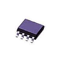
Package / Case
SOIC-8
Minimum Operating Temperature
0 C
Operating Supply Voltage
2.5 V, 5.5 V
Operating Temperature
0 C to + 70 C
Lead Free Status / Rohs Status
No
Available stocks
Company
Part Number
Manufacturer
Quantity
Price
Company:

Part Number:
IS24C02-3G
Manufacturer:
XILINX
Quantity:
10


IS24C01 IS24C02 IS24C04 IS24C08
PIN CONFIGURATION
8-Pin DIP and SOIC
8 Pin TSSOP (1K, 2K, 4K and 8K)
8-Pin MSOP (1K, 2K)
Integrated Silicon Solution, Inc. — www.issi.com —
Rev. F
03/24/04
PIN DESCRIPTIONS
SCL
This input clock pin is used to synchronize the data
transfer to and from the device.
SDA
The SDA is a Bi-directional pin used to transfer addresses and data
into and out of the device. The SDA pin is an open drain output and
can be wire-Ored with other open drain or open collector outputs.
The SDA bus requires a pullup resistor to Vcc.
A0, A1, A2
The A0, A1 and A2 are the device address inputs. The IS24C01 and
IS24C02 use the A0, A1, and A2 for hardware addressing and a
total of 8 devices may be used on a single bus system.
A0-A2
SDA
SCL
WP
Vcc
GND
GND
A0
A1
A2
1
2
3
4
Address Inputs
Serial Address/Data I/O
Serial Clock Input
Write Protect Input
Power Supply
Ground
8
7
6
5
VCC
WP
SCL
SDA
1-800-379-4774
The IS24C04 uses A1 and A2 pins for hardwire addressing and
a total of four devices may be addressed on a single bus system.
The A0 pin is not used by IS24C04. This pin can be left floating
or tied to GND or Vcc.
The IS24C08 only use A2 input for hardwire addressing and a
total of two devices may be addressed on a single bus system.
The A0 and A1 pins are not used by IS24C08. They may be left
floating or tied to either GND or Vcc.
These pins are not used by IS24C16. A0 and A1 may be left
floating or tied to either GND or Vcc. A2 should be tied to either
GND or Vcc.
WP
WP is the Write Protect pin. On the 24C01, 24C02, IS24C04
and 24C08, if the WP pin is tied to V
becomes Write Protected (Read only). On the 24C16, if the
WP pin is tied to Vcc the upper half array becomes Write
Protected (Read only). When WP is tied to GND or left
floating normal read/write operations are allowed to the
device.
IS24C16
CC
ISSI
the entire array
®
3
Related parts for IS24C02-3G
Image
Part Number
Description
Manufacturer
Datasheet
Request
R

Part Number:
Description:
EEPROM 2.5V 2Kb
Manufacturer:
ISSI, Integrated Silicon Solution Inc
Datasheet:

Part Number:
Description:
IC SRAM 256KBIT 12NS 28SOJ
Manufacturer:
ISSI, Integrated Silicon Solution Inc
Datasheet:

Part Number:
Description:
IC SDRAM 16MBIT 143MHZ 50TSOP
Manufacturer:
ISSI, Integrated Silicon Solution Inc
Datasheet:

Part Number:
Description:
IC SRAM 1MBIT 12NS 44TSOP
Manufacturer:
ISSI, Integrated Silicon Solution Inc
Datasheet:

Part Number:
Description:
IC SRAM 1MBIT 10NS 44TSOP
Manufacturer:
ISSI, Integrated Silicon Solution Inc
Datasheet:

Part Number:
Description:
IC SRAM 1MBIT 12NS 32SOJ
Manufacturer:
ISSI, Integrated Silicon Solution Inc
Datasheet:

Part Number:
Description:
IC SRAM 1MBIT 12NS 32TSOP
Manufacturer:
ISSI, Integrated Silicon Solution Inc
Datasheet:

Part Number:
Description:
IC SRAM 1MBIT 35NS 32TSOP
Manufacturer:
ISSI, Integrated Silicon Solution Inc
Datasheet:

Part Number:
Description:
IC SRAM 1MBIT 35NS 32SOP
Manufacturer:
ISSI, Integrated Silicon Solution Inc
Datasheet:

Part Number:
Description:
IC SRAM 1MBIT 12NS 32SOJ
Manufacturer:
ISSI, Integrated Silicon Solution Inc
Datasheet:

Part Number:
Description:
IC SRAM 1MBIT 12NS 44SOJ
Manufacturer:
ISSI, Integrated Silicon Solution Inc
Datasheet:

Part Number:
Description:
IC SDRAM 64MBIT 143MHZ 54TSOP
Manufacturer:
ISSI, Integrated Silicon Solution Inc
Datasheet:

Part Number:
Description:
IC SRAM 4MBIT 10NS 44TSOP
Manufacturer:
ISSI, Integrated Silicon Solution Inc
Datasheet:

Part Number:
Description:
IC SRAM 4MBIT 55NS 32STSOP
Manufacturer:
ISSI, Integrated Silicon Solution Inc
Datasheet:

Part Number:
Description:
IC SDRAM 256MBIT 143MHZ 54TSOP
Manufacturer:
ISSI, Integrated Silicon Solution Inc
Datasheet: