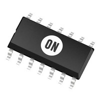
MC74AC74D ON Semiconductor, MC74AC74D Datasheet - Page 3

MC74AC74D
Manufacturer Part Number
MC74AC74D
Description
Flip Flops 2-6V CMOS Dual
Manufacturer
ON Semiconductor
Datasheet
1.MC74AC74DR2G.pdf
(12 pages)
Specifications of MC74AC74D
Number Of Circuits
2
Logic Family
74AC
Logic Type
D-Type Edge Triggered Flip-Flop
Polarity
Inverting/Non-Inverting
Input Type
Single-Ended
Propagation Delay Time
14 ns
High Level Output Current
- 24 mA
Supply Voltage (max)
6 V
Maximum Operating Temperature
+ 85 C
Mounting Style
SMD/SMT
Package / Case
SOIC-14
Minimum Operating Temperature
- 40 C
Supply Voltage (min)
2 V
Dc
08+
Lead Free Status / Rohs Status
No RoHS Version Available
Available stocks
Company
Part Number
Manufacturer
Quantity
Price
Part Number:
MC74AC74DG
Manufacturer:
ON/安森美
Quantity:
20 000
Company:
Part Number:
MC74AC74DR2
Manufacturer:
MOTOROLA
Quantity:
4 453
Part Number:
MC74AC74DR2
Manufacturer:
ON/安森美
Quantity:
20 000
Company:
Part Number:
MC74AC74DTR2
Manufacturer:
ON Semiconductor
Quantity:
1 600
Company:
Part Number:
MC74AC74DTR2G
Manufacturer:
TI
Quantity:
4 600
RECOMMENDED OPERATING CONDITIONS
V
V
t
t
T
T
I
I
1. V
2. V
DC CHARACTERISTICS
V
V
V
V
I
I
I
I
*All outputs loaded; thresholds on input associated with output under test.
†Maximum test duration 2.0 ms, one output loaded at a time.
NOTE:
r
r
OH
OL
IN
OLD
OHD
CC
, t
, t
A
J
CC
in
IH
IL
OH
OL
Symbol
Symbol
, V
f
f
in
in
out
from 30% to 70% V
from 0.8 V to 2.0 V; see individual Data Sheets for devices that differ from the typical input rise and fall times.
I
IN
and I
Minimum High Level
Input Voltage
Maximum Low Level
Input Voltage
Minimum High Level
Output Voltage
Maximum Low Level
Output Voltage
Maximum Input
Leakage Current
†Minimum Dynamic
Maximum Quiescent
Supply Current
Supply Voltage
DC Input Voltage, Output Voltage (Ref. to GND)
Input Rise and Fall Time (Note )
′AC Devices except Schmitt Inputs
Input Rise and Fall Time (Note )
′ACT Devices except Schmitt Inputs
Junction Temperature (PDIP)
Operating Ambient Temperature Range
Output Current − High
Output Current − Low
Output Current
CC
@ 3.0 V are guaranteed to be less than or equal to the respective limit @ 5.5 V V
CC
; see individual Data Sheets for devices that differ from the typical input rise and fall times.
Parameter
Parameter
http://onsemi.com
V
3.0
4.5
5.5
3.0
4.5
5.5
3.0
4.5
5.5
3.0
4.5
5.5
3.0
4.5
5.5
3.0
4.5
5.5
5.5
5.5
5.5
5.5
(V)
CC
3
0.002
0.001
0.001
V
V
V
V
V
2.25
2.75
2.25
2.75
2.99
4.49
5.49
Typ
1.5
1.5
T
−
−
−
−
−
−
−
−
−
−
CC
CC
CC
CC
CC
A
74AC
′ACT
= +25°C
′AC
@ 3.0 V
@ 4.5 V
@ 5.5 V
@ 4.5 V
@ 5.5 V
3.15
3.85
1.35
1.65
2.56
3.86
4.86
0.36
0.36
0.36
±0.1
2.1
0.9
2.9
4.4
5.4
0.1
0.1
0.1
4.0
Guaranteed Limits
−
−
−40°C to
Min
−40
2.0
4.5
74AC
+85°C
T
3.15
3.85
1.35
1.65
2.46
3.76
4.76
0.44
0.44
0.44
±1.0
0
−
−
−
−
−
−
−
−
−75
2.1
0.9
2.9
4.4
5.4
0.1
0.1
0.1
75
40
A
=
Typ
150
CC
5.0
5.0
8.0
40
25
10
25
−
−
−
−
.
Unit
mA
mA
mA
mA
V
V
V
V
V
V
Max
V
140
−24
V
or V
V
or V
I
*V
I
I
*V
I
V
V
V
V
6.0
5.5
OUT
OH
OUT
OL
85
24
CC
−
−
−
−
−
OUT
OUT
I
OLD
OHD
IN
IN
IN
= V
= V
CC
CC
Conditions
= V
= V
= −50 mA
= 50 mA
= 1.65 V Max
= 0.1 V
= 0.1 V
CC
= 3.85 V Min
− 0.1 V
− 0.1 V
CC
IL
IL
, GND
−12 mA
−24 mA
−24 mA
or V
or V
12 mA
24 mA
24 mA
or GND
Unit
ns/V
ns/V
mA
mA
°C
°C
V
V
IH
IH


