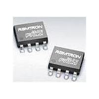
FM24CL64-G Ramtron, FM24CL64-G Datasheet

FM24CL64-G
Specifications of FM24CL64-G
Available stocks
Related parts for FM24CL64-G
FM24CL64-G Summary of contents
Page 1
... A1 A2 VSS caused by higher than VSS Pin Names A0-A2 SDA SCL WP VSS VDD Ordering Information FM24CL64-G FM24CL64-GTR FM24CL64-DG FM24CL64-DGTR FM24CL64-S * FM24CL64-STR * † Grade 3 AEC-Q100 Qualified * End of life. Last time buy June 2009. 1850 Ramtron Drive, Colorado Springs, CO 80921 VDD SCL 3 6 SDA ...
Page 2
... When WP is low, all addresses may be written. This pin is pulled down internally. VDD Supply Supply Voltage: 2.7V to 3.6V VSS Supply Ground Rev. 3.4 Feb. 2011 Address Latch Converter Figure 1. FM24CL64 Block Diagram FM24CL64 2,048 x 32 FRAM Array 8 Data Latch Page ...
Page 3
... This is explained in more detail in the interface section below. Users expect several obvious system benefits from the FM24CL64 due to its fast write cycle and high endurance as compared with EEPROM. However there are less obvious benefits as well. For example ...
Page 4
... Slave Address The first byte that the FM24CL64 expects after a start condition is the slave address. As shown in Figure 4, the slave address contains the device type, the device select address bits, and a bit that specifies if the transaction is a read or a write ...
Page 5
... After the address information has been transmitted, data transfer between the bus master and the FM24CL64 can begin. For a read operation the FM24CL64 will place 8 data bits on the bus then wait for an acknowledge from the master. If the acknowledge occurs, the FM24CL64 will transfer the next sequential byte ...
Page 6
... Acknowledge Figure 6. Multiple Byte Write There are four ways to properly terminate a read operation. Failing to properly terminate the read will most likely create a bus contention as the FM24CL64 attempts to read out additional data onto the bus. The four valid methods are: 1. The bus master issues a no-acknowledge in the ...
Page 7
... By Master S By FM24CL64 Start Address By Master S Slave Address By FM24CL64 Start By Master S Slave Address 0 A Address MSB By FM24CL64 Rev. 3.4 Feb. 2011 set The operation is now a current address read. Address Slave Address 1 A Data Byte Acknowledge Data Figure 7. Current Address Read Acknowledge 1 A ...
Page 8
... Std JESD22-A115-A) =2.7V to 3.65V unless otherwise specified) DD Min 2.7 -0 other inputs -0.3V Stop command issued FM24CL64 Ratings -1.0V to +5.0V -1.0V to +5.0V and V < V +1. -55°C to +125°C 300° C 4kV 300V MSL-1 Typ Max Units Notes 3. µA 150 µ ...
Page 9
... DD Max Units Notes FM24CL64 Max Min Max Units Notes 400 0 1000 kHz 1 0.6 µs 0.4 µs 0.9 0.55 µs 0.5 µs 0.25 µs 0.25 µ 100 ns 300 300 ns 2 300 100 ...
Page 10
... Write Bus Timing SCL t SU:STO SDA Start Data Retention (V = 2.7V to 3.65V, 85°C) DD Parameter Data Retention Rev. 3.4 Feb. 2011 t HIGH 1/fSCL t AA Stop Start t HD:DAT t t SU:DAT HD:STA Stop Start Min Units 45 Years FM24CL64 LOW t HD:DAT t SU:DAT t DH Acknowledge t AA Acknowledge Notes Page ...
Page 11
... SOIC Package Marking Scheme Legend: XXXX= part number, P= package type LLLLLLL= lot code XXXXXXX-P RIC=Ramtron Int’l Corp, YY=year, WW=work week LLLLLLL RICYYWW Example: FM24CL64, “Green” SOIC package, Year 2004, Work Week 39 FM24CL64-G A40003G1 RIC0439 Rev. 3.4 Feb. 2011 FM24CL64 Page ...
Page 12
... Legend: R=Ramtron, G=”green” TDFN package, XXXX=base part number LLLL= lot code, RGXXXX YY=year, WW=work week LLLL YYWW Example: “Green” TDFN package, FM24CL64, Lot 0003, Industrial temperature, Year 2005, Work Week 14 RG4L64 0003 0514 Rev. 3.4 Feb. 2011 Exposed metal pad. ...
Page 13
... Changed TDFN Package Marking Scheme. Marked –S ordering number as “not recommended for new designs”. Added tape and reel ordering information. Added last time buy notice on –S ordering number. Added notation that –G parts are Grade 3. Not recommended for new designs. Alternative: FM24CL64B. FM24CL64 Page ...


