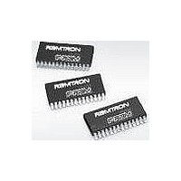
FM18L08-70-S Ramtron, FM18L08-70-S Datasheet - Page 6

FM18L08-70-S
Manufacturer Part Number
FM18L08-70-S
Description
F-RAM 256K (32Kx8) 70ns 3V
Manufacturer
Ramtron
Datasheet
1.FM18L08-70-TG.pdf
(13 pages)
Specifications of FM18L08-70-S
Memory Size
256 KB
Organization
32 K x 8
Interface
Parallel
Access Time
70 ns
Operating Supply Voltage
3 V to 3.6 V
Operating Temperature Range
- 40 C to + 85 C
Package / Case
SOIC-28
Mounting Style
SMD/SMT
Lead Free Status / Rohs Status
No
Available stocks
Company
Part Number
Manufacturer
Quantity
Price
Company:
Part Number:
FM18L08-70-S
Manufacturer:
RAMTRON
Quantity:
5 510
Part Number:
FM18L08-70-S
Manufacturer:
RAMTRON
Quantity:
20 000
Company:
Part Number:
FM18L08-70-SG
Manufacturer:
RAMTRON
Quantity:
15 040
Company:
Part Number:
FM18L08-70-SG
Manufacturer:
RAMRON
Quantity:
77
Part Number:
FM18L08-70-SG
Manufacturer:
RAMTRON
Quantity:
20 000
Company:
Part Number:
FM18L08-70-SGTR
Manufacturer:
ON
Quantity:
2 000
Part Number:
FM18L08-70-SGTR
Manufacturer:
RAMTRON
Quantity:
20 000
Electrical Specifications
Absolute Maximum Ratings
Stresses above those listed under Absolute Maximum Ratings may cause permanent damage to the device. This is a stress rating
only, and the functional operation of the device at these or any other conditions above those listed in the operational section of this
specification is not implied. Exposure to absolute maximum ratings conditions for extended periods may affect device reliability.
DC Operating Conditions (T
Notes
1.
2.
3.
4.
Rev. 3.5
Sept. 2009
V
I
I
I
I
I
V
V
V
V
Symbol
DD
SB1
SB2
LI
LO
DD
IH
IL
OH
OL
V
V
V
V
DD
DD
DD
IN
, V
= 3.65V, /CE cycling at minimum cycle time. All inputs at CMOS levels, all outputs unloaded.
= 3.65V, /CE at V
= 3.65V, /CE at V
Symbol
T
OUT
V
T
V
V
LEAD
STG
ESD
DD
IN
Power Supply
V
Standby Current – TTL
Standby Current – CMOS
Input Leakage Current
Output Leakage Current
Input High Voltage
Input Low Voltage
Output High Voltage (
Output Low Voltage (
between V
DD
Supply Current – Active
DD
IH
DD
and V
, All other pins at TTL levels.
Power Supply Voltage with respect to V
Voltage on any signal pin with respect to V
Storage temperature
Lead temperature (Soldering, 10 seconds)
Electrostatic Discharge Voltage
Package Moisture Sensitivity Level
Parameter
, All other pins at CMOS levels.
- Human Body Model
- Machine Model
A
SS
= -40 C to + 85 C, V
.
I
I
OL
OH
= 3.2 mA)
= -1.0 mA)
Description
(JEDEC Std JESD22-A115-A)
(JEDEC Std JESD22-A114-B)
DD
= 3.0V to 3.65V)
Min
-0.5
3.0
2.0
2.4
-
-
-
-
SS
SS
Typ
7
7
-1.0V to +5.0V and V
V
MSL-1 (SOIC/DIP)
DD
Max
3.65
-55 C to +125 C
400
0.8
0.4
MSL-2 (TSOP)
15
15
10
10
-1.0V to +5.0V
-
+ 0.5
< V
Ratings
300 C
400V
4kV
DD
+1V
Units
mA
V
V
V
V
V
A
A
A
A
IN
FM18L08
Notes
1
2
3
4
4
6 of 13


