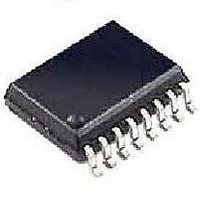
DG612DY Vishay, DG612DY Datasheet - Page 8

DG612DY
Manufacturer Part Number
DG612DY
Description
Analog Switch ICs High-Speed Switch
Manufacturer
Vishay
Datasheet
1.DG611DY-T1-E3.pdf
(10 pages)
Specifications of DG612DY
Number Of Switches
4
Switch Configuration
SPST
On Resistance (max)
18 Ohms
On Time (max)
50 ns
Off Time (max)
35 ns
Off Isolation (typ)
74 dB
Bandwidth
500 MHz
Supply Voltage (max)
21 V
Supply Voltage (min)
5 V
Supply Current
5 uA
Maximum Power Dissipation
600 mW
Maximum Operating Temperature
+ 85 C
Mounting Style
SMD/SMT
Package / Case
SOIC-16
Minimum Operating Temperature
- 40 C
Number Of Lines (input / Output)
4 / 4
Off State Leakage Current (max)
20 nA
Lead Free Status / Rohs Status
No RoHS Version Available
Available stocks
Company
Part Number
Manufacturer
Quantity
Price
Company:
Part Number:
DG612DY-E3
Manufacturer:
Vishay
Quantity:
669
Company:
Part Number:
DG612DY-T1-E3
Manufacturer:
Vishay
Quantity:
4 217
Part Number:
DG612DY-T1-E3
Manufacturer:
VISHAY/威世
Quantity:
20 000
DG611, DG612, DG613
Vishay Siliconix
TEST CIRCUITS
APPLICATIONS
High-Speed Sample-and-Hold
In a fast sample-and-hold application, the analog switch
characteristics are critical. A fast switch reduces aperture
uncertainty. A low charge injection eliminates offset (step)
errors. A low leakage reduces droop errors. The CLC111, a
fast input buffer, helps to shorten acquisition and settling
times. A low leakage, low dielectric absorption hold capacitor
must
polypropylene are good choices. The JFET output buffer
reduces droop due to its low input bias current.
(see figure 5.)
www.vishay.com
8
V
be
g
Analog
used.
Input
5 V
R
g
Figure 3. Charge Injection
Polycarbonate,
S
IN
GND
+ 5 V
V
L
75
5 V Control
+ 15 V
- 3 V
V+
V-
Input Buffer
D
CLC111
polystyrene
Figure 5. High-Speed Sample-and-Hold
C
1 nF
V
L
O
S
IN
and
1
/
4
+ 5 V
DG611
X
Pixel-Rate Switch
Windows, picture-in-picture, title overlays are economically
generated using a high-speed analog switch such as the
DG613. For this application the two video sources must be
sync locked. The glitch-less analog switch eliminates halos.
(see figure 6.)
GaAs FET Drivers
Figure 7 illustrates a high-speed GaAs FET driver. To turn
the GaAs FET on 0 V are applied to its gate via S
to turn it off, - 8 V are applied via S
low-power driver is especially suited for applications that
require a large number of RF switches, such as phased array
radars.
C = RF bypass
TA LK
+ 12 V
- 5 V
D
Isolation = 20 log
V
S
R
C
650 pF Polystyrene
g
HOLD
= 50
1 V, 4 V
1 V, 4 V
Output Buffer
+
-
LF356
NC
Figure 4. Crosstalk
V
V
S
O
C
S
IN
S
IN
+ 5 V
1
2
V
1
2
GND
L
S11-0154-Rev. I, 31-Jan-11
Document Number: 70057
± 5 V Output
to A/D
- 3 V
2
V-
. This high-speed,
+ 15 V
V+
D
D
1
2
C
1
C
, whereas
50
R
V
O
L


