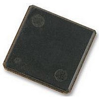
H5PS1G83EFR-S6C HYNIX SEMICONDUCTOR, H5PS1G83EFR-S6C Datasheet - Page 40

H5PS1G83EFR-S6C
Manufacturer Part Number
H5PS1G83EFR-S6C
Description
58T1895
Manufacturer
HYNIX SEMICONDUCTOR
Datasheet
1.H5PS1G83EFR-S6C.pdf
(44 pages)
Specifications of H5PS1G83EFR-S6C
Memory Type
SDRAM
Memory Configuration
128M X 8
Access Time
15ns
Memory Case Style
FBGA
No. Of Pins
60
Operating Temperature Range
0°C To +85°C
Memory Size
1 Gbit
Rohs Compliant
Yes
Available stocks
Company
Part Number
Manufacturer
Quantity
Price
Company:
Part Number:
H5PS1G83EFR-S6C
Manufacturer:
HYNIX
Quantity:
4 000
Part Number:
H5PS1G83EFR-S6C
Manufacturer:
HYNIX/海力士
Quantity:
20 000
Company:
Part Number:
H5PS1G83EFR-S6C-C
Manufacturer:
HYNIX
Quantity:
9 500
Company:
Part Number:
H5PS1G83EFR-S6C-C
Manufacturer:
HYNIX
Quantity:
135
Company:
Part Number:
H5PS1G83EFR-S6C-C-6Z
Manufacturer:
HYNIX
Quantity:
5 361
Rev. 0.4 / Nov 2008
36. These parameters are specified per their average values, however it is understood that the following
relationship between the average timing and the absolute instantaneous timing holds at all times. (Min and
max of SPEC values are to be used for calculations in the table below.)
Example: For DDR2-667, tCH (abs), min = (0.48 x 3000 ps) - 125 ps = 1315 ps
37. tHP is the minimum of the absolute half period of the actual input clock. tHP is an input parameter but
not an input specification parameter. It is used in conjunction with tQHS to derive the DRAM output timing
tQH.
The value to be used for tQH calculation is determined by the following equation;
tHP = Min (tCH (abs), tCL (abs)),
where,
tCH (abs) is the minimum of the actual instantaneous clock HIGH time;
tCL (abs) is the minimum of the actual instantaneous clock LOW time;
38. tQHS accounts for:
1) The pulse duration distortion of on-chip clock circuits, which represents how well the actual tHP at the
input is transferred to the output; and
2) The worst case push-out of DQS on one transition followed by the worst case pull-in of DQ on the next
transition, both of which are independent of each other, due to data pin skew, output pattern effects, and
p-channel to n-channel variation of the output drivers
39. tQH = tHP ? tQHS, where:
tHP is the minimum of the absolute half period of the actual input clock; and
tQHS is the specification value under the max column.
{The less half-pulse width distortion present, the larger the tQH value is; and the larger the valid data eye
will be.}
Examples:
1) If the system provides tHP of 1315 ps into a DDR2-667 SDRAM, the DRAM provides tQH of 975 ps min-
imum.
2) If the system provides tHP of 1420 ps into a DDR2-667 SDRAM, the DRAM provides tQH of 1080 ps
minimum.
40. When the device is operated with input clock jitter, this parameter needs to be derated by the actual
tERR(6-10per) of the input clock. (output deratings are relative to the SDRAM input clock.)
For example, if the measured jitter into a DDR2-667 SDRAM has tERR(6-10per),min = - 272 ps and
tERR(6-10per), max = + 293 ps, then tDQSCK, min (derated) = tDQSCK, min - tERR(6-10per),max = -
400 ps - 293 ps = - 693 ps and tDQSCK, max (derated) = tDQSCK, max - tERR(6-10per),min = 400 ps +
Absolute clock HIGH pulse width
Absolute clock LOW pulse width
Absolute clock period
Parameter
Symbol
tCK (abs)
tCH (abs)
tCL (abs)
tCH (avg), min * tCK (avg), min +
tCL (avg), min * tCK (avg), min +
tCK (avg), min + tJIT (per), min
tJIT (per), min
tJIT (per), min
min
tCH (avg), max * tCK (avg), max
tCK (avg), max + tJIT (per), max
tCL (avg), max * tCK (avg), max
+ tJIT (per), max
+ tJIT (per), max
max
H5PS1G43EFR
H5PS1G83EFR
H5PS1G63EFR
Units
ps
ps
ps
40


