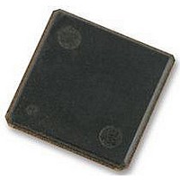
H5PS5162FFR-S6C HYNIX SEMICONDUCTOR, H5PS5162FFR-S6C Datasheet - Page 13

H5PS5162FFR-S6C
Manufacturer Part Number
H5PS5162FFR-S6C
Description
58T1896
Manufacturer
HYNIX SEMICONDUCTOR
Datasheet
1.H5PS5162FFR-S6C.pdf
(39 pages)
Specifications of H5PS5162FFR-S6C
Memory Type
SDRAM
Memory Configuration
32M X 16
Memory Case Style
FBGA
No. Of Pins
84
Operating Temperature Range
0°C To +85°C
Memory Size
512 Mbit
Voltage Vcc
1.8V
Rohs Compliant
Yes
Available stocks
Company
Part Number
Manufacturer
Quantity
Price
Company:
Part Number:
H5PS5162FFR-S6C
Manufacturer:
HYNIX
Quantity:
9 500
Company:
Part Number:
H5PS5162FFR-S6C
Manufacturer:
HYNIX
Quantity:
2 000
Company:
Part Number:
H5PS5162FFR-S6C
Manufacturer:
ST
Quantity:
40
Company:
Part Number:
H5PS5162FFR-S6C
Manufacturer:
HYNIX
Quantity:
4 000
Part Number:
H5PS5162FFR-S6C
Manufacturer:
HYNIX/海力士
Quantity:
20 000
Rev. 1.0 / July. 2008
3.3.3 OCD default characteristics
Output impedance
Output impedance step size for OCD calibration
Pull-up and pull-down mismatch
Output slew rate
Note
1. Absolute Specifications ( Toper; VDD = +1.8V ±0.1V, VDDQ = +1.8V ±0.1V). DRAM I/O specifications for
Device Operation & Timing Diagram of DDR2 for the Full Strength Default Driver Characteristics.
2. Impedance measurement condition for output source dc current: VDDQ=1.7V; VOUT=1420mV; (VOUT-VDDQ)/Ioh
must be less than 23.4 ohms for values of VOUT between VDDQ and VDDQ-280mV. Impedance measurement
condition for output sink dc current: VDDQ = 1.7V; VOUT = 280mV; VOUT/Iol must be less than 23.4 ohms for
values of VOUT between 0V and 280mV.
3. Mismatch is absolute value between pull-up and pull-dn, both are measured at same temperature and voltage.
4. Slew rate measured from vil(ac) to vih(ac).
5. The absolute value of the slew rate as measured from DC to DC is equal to or greater than the slew rate as
6. This represents the step size when the OCD is near 18 ohms at nominal conditions across all process corners/
7. DRAM output slew rate specification applies to 400 , 533 and 667 MT/s speed bins.
8. Timing skew due to DRAM output slew rate mis-match between DQS / DQS and associated DQs is included in
measured from AC to AC. This is guaranteed by design and characterization.
timing,voltage, and slew rate are no longer applicable if OCD is changed from default settings. Please refer to the
Output Slew rate load:
variations and represents only the DRAM uncertainty. A 0 ohm value(no calibration) can only be achieved if the
OCD impedance is 18 ohms +/- 0.75 ohms under nominal conditions.
tDQSQ and tQHS specification.
Description
Output
(Vout)
Parameter
Sout
VTT
25 ohms
See full strength default
1.5
Reference
Min
driver characteristics
0
0
point
Nom
-
H5PS5162FFR series
1.5
Max
4
5
ohms
ohms
ohms
V/ns
Unit
Release
1,4,5,6,7,8
1,2,3
Notes
1
6
13


