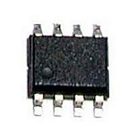
A25L020O-F AMIC, A25L020O-F Datasheet - Page 4

A25L020O-F
Manufacturer Part Number
A25L020O-F
Description
58T1303
Manufacturer
AMIC
Datasheet
1.A25L020-F.pdf
(44 pages)
Specifications of A25L020O-F
Memory Type
Flash
Memory Size
2Mbit
Memory Configuration
2M X 1
Interface Type
Serial, SPI
Clock Frequency
100MHz
Supply Voltage Range
2.7V To 3.6V
Memory Case Style
SOIC
No. Of Pins
8
Rohs Compliant
Yes
Available stocks
Company
Part Number
Manufacturer
Quantity
Price
Part Number:
A25L020O-F/Q
Manufacturer:
AMIC
Quantity:
20 000
Pin Descriptions
Notes:
1. The DIO is also used as an output pin when the Fast
2. The DO is also used as an input pin when the Fast
SIGNAL DESCRIPTION
Serial Data Output (DO). This output signal is used to
transfer data serially out of the device. Data is shifted out on
the falling edge of Serial Clock (C).
The DO pin is also used as an input pin when the Fast Read
Dual Input-Output instruction is executed.
Serial Data Input (DIO). This input signal is used to transfer
data serially into the device. It receives instructions,
addresses, and the data to be programmed. Values are
latched on the rising edge of Serial Clock (C).
The DIO pin is also used as an output pin when the Fast
Read Dual Output instruction and the Fast Read Dual
Input-Output instruction are executed.
Serial Clock (C). This input signal provides the timing of the
serial interface. Instructions, addresses, or data present at
Serial Data Input (DIO) are latched on the rising edge of
Serial Clock (C). Data on Serial Data Output (DO) changes
after the falling edge of Serial Clock (C).
Chip Select (
is deselected and Serial Data Output (DO) is at high
impedance. Unless an internal Program, Erase or Write
(December, 2010, Version 1.6)
C
DIO
DO
V
V
HOLD
S
W
CC
SS
Read Dual Output instruction and the Fast Read Dual
Input-Output instruction are executed.
Read Dual Input-Output instruction is executed.
Pin No.
S
). When this input signal is High, the device
Serial Clock
Serial Data Input
Serial Data Output
Chip Select
Write Protect
Hold
Supply Voltage
Ground
Description
1
2
3
Status Register cycle is in progress, the device will be in the
Standby mode (this is not the Deep Power-down mode).
Driving Chip Select (
the active power mode.
After Power-up, a falling edge on Chip Select (
prior to the start of any instruction.
Hold (
any
deselecting the device.
During the Hold condition, the Serial Data Output (DO) is
high impedance, and Serial Data Input (DIO) and Serial
Clock (C) are Don’t Care. To start the Hold condition, the
device must be selected, with Chip Select (
Write Protect (
to freeze the size of the area of memory that is protected
against program or erase instructions (as specified by the
values in the BP2, BP1, and BP0 bits of the Status Register).
A25L020/A25L010/A25L512 Series
serial
HOLD
communications
). The Hold (
W
HOLD
). The main purpose of this input signal is
DIO
W
C
S
S
Logic Symbol
) Low enables the device, placing it in
AMIC Technology Corp.
V
HOLD
V
A25L020/
A25L010/
A25L512
SS
CC
with
) signal is used to pause
the
S
DO
device
) driven Low.
S
) is required
without


