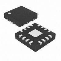
MAX4855ETE+ Maxim Integrated Products, MAX4855ETE+ Datasheet - Page 2

MAX4855ETE+
Manufacturer Part Number
MAX4855ETE+
Description
IC MULTIPLEXER DUAL SPDT 16TQFN
Manufacturer
Maxim Integrated Products
Datasheet
1.MAX4855ETET.pdf
(10 pages)
Specifications of MAX4855ETE+
Function
Multiplexer
Circuit
2 x SPDT
On-state Resistance
7.5 Ohm
Voltage Supply Source
Single Supply
Voltage - Supply, Single/dual (±)
2 V ~ 5.5 V
Current - Supply
1µA
Operating Temperature
-40°C ~ 85°C
Mounting Type
Surface Mount
Package / Case
16-TQFN Exposed Pad
Lead Free Status / RoHS Status
Lead free / RoHS Compliant
0.75Ω, Dual SPDT Audio Switch with
Integrated Comparators
ABSOLUTE MAXIMUM RATINGS
V
NO_, NC_, COM_, COUT_ (Note 1) ...............-0.3V to (V
COUT_ Continuous Current...................................................±20mA
Closed Switch Continuous Current COM_, NO_, NC_.......±300mA
Peak Current COM_, NO_, NC_
Peak Current COM_, NO_, NC_
ELECTRICAL CHARACTERISTICS
(V
wise noted.) (Note 2)
Stresses beyond those listed under “Absolute Maximum Ratings” may cause permanent damage to the device. These are stress ratings only, and functional
operation of the device at these or any other conditions beyond those indicated in the operational sections of the specifications is not implied. Exposure to
absolute maximum rating conditions for extended periods may affect device reliability.
2
Note 1: Signals on NO, NC, or COM exceeding V
Supply Voltage
Supply Current
ANALOG SWITCH
Analog Signal Range
On-Resistance (Note 3)
On-Resistance Match
Between Channels
(Notes 3, 4)
On-Resistance Flatness
(Note 5)
NO_/NC_ Off-Leakage
Current (Note 2)
COM_ On-Leakage
Current (Note 2)
DYNAMIC CHARACTERISTICS
Turn-On Time
CC
CC
(pulsed at 1ms, 50% duty cycle) ....................................±400mA
(pulsed at 1ms, 10% duty cycle) ....................................±500mA
, IN_, CIN_ to GND ..............................................-0.3V to +6.0V
_______________________________________________________________________________________
= +2.7V to +5.5V, T
PARAMETER
clamped by an internal diode. Limit forward-diode current to maximum current rating.
A
= -40°C to +85°C, unless otherwise noted. Typical values are at V
SYMBOL
V
V
V
∆R
R
R
V
COM_
I
I
I
t
NO_
NC_
FLAT
OFF
CC
ON
ON
CC
ON
ON
,
,
V
V
100mA, V
to V
V
V
V
100mA, V
0.75V, 1.5V, 1.75V
V
1V or 4.5V, V
1V
V
1V, 4.5V, or floating; V
= 1V, 4.5V, or floating
V
1.5V, R
(Figure 1)
CC
CC
CC
NC_
CC
CC
CC
CC
CC
= 5.5V, V
= 2.7V, I
= 2.7V, I
= 2.7V, I
= 5.5V, V
= 5.5V; V
= 2.7V, V
or V
L
= 300Ω, C
NC_
NO_
NC_
CC
CC
COM_
COM_
COM
COM_
IN_
NC_
NC_
NO_
or V
or V
= 1.5V
or GND are clamped by internal diodes. Signals on IN exceeding GND are
+ 0.3V)
= 0V or V
NO_
NO_
= 100mA,
or V
or V
or V
= 4.5V or
=
=
L
CONDITIONS
= 50pF
COM_
NO_
NO_
NC_
= 0V
=
CC
=
=
=
Continuous Power Dissipation (T
Operating Temperature Range................................-40°C to +85°C
Junction Temperature ...........................................................+150°C
Storage Temperature Range .................................-65°C to +150°C
Lead Temperature (soldering, 10s)......................................+300°C
T
T
T
T
T
T
T
T
T
T
T
T
16-Pin Thin QFN (derate 20.8mW/°C above +70°C) .....1667mW
A
A
A
A
A
A
A
A
A
A
A
A
= +25°C
= -40°C to +85°C
= +25°C
= -40°C to +85°C
= +25°C
= -40°C to +85°C
= +25°C
= -40°C to +85°C
= +25°C
= -40°C to +85°C
= +25°C
= -40°C to +85°C
CC
= +3.0V, T
MIN
-10
-15
-2
-2
2
0
A
= +70°C)
0.075
TYP
0.75
0.18
40
A
5
= +25°C, unless other-
0.120
0.135
0.275
MAX
V
+10
+15
100
5.5
1.1
0.3
10
+2
+2
60
CC
1
UNITS
µA
nA
nA
ns
Ω
Ω
Ω
V
V


