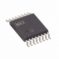
MAX14753EUE+ Maxim Integrated Products, MAX14753EUE+ Datasheet

MAX14753EUE+
Specifications of MAX14753EUE+
Related parts for MAX14753EUE+
MAX14753EUE+ Summary of contents
Page 1
... EN Voltage Defines Logic Level of S0, S1, and S2 ♦ Low I DD ♦ Overvoltage/Undervoltage Clamp Through Protection Diodes ♦ Break-Before-Make Operation ♦ Pin Compatible with Industry-Standard DG408/DG409 Applications PART MAX14752EUE+ MAX14753EUE+ + Denotes a lead(Pb)-free/RoHS-compliant package. INA0 INA1 INA2 INA3 OUT INB0 INB1 INB2 INB3 ...
Page 2
Analog Multiplexers ABSOLUTE MAXIMUM RATINGS .............................................................-0.3V to +72V DD SS GND to V ..............................................................-0. EN, S0, S1 GND ................................................................. ..............................-0.3V to the lesser of (+12V and V IN_, INA_, ...
Page 3
DC ELECTRICAL CHARACTERISTICS–DUAL SUPPLIES (continued +35V -35V 0V GND PARAMETER SYMBOL Output Off-Leakage Current I OUT(OFF) Input Off-Leakage Current I IN(OFF) LOGIC (EN, S0, S1, S2) EN Input Voltage Low V ...
Page 4
Analog Multiplexers DC ELECTRICAL CHARACTERISTICS–SINGLE SUPPLY (V = +70V 0V +3.3V GND EN PARAMETER SYMBOL On-Resistance I OUT(OFF) OUT, OUTA, OUTB Off-Leakage I OUTA(OFF Current I OUTB(OFF) On-Input ...
Page 5
1µ MAX14752 MAX14753 IN_ INA_ INB_ GND SS 1µ Figure 1. On-Resistance V DD 1μ MAX14752 I IN(OFF) I MAX14753 INA(OFF) IN_ I INB(OFF) INA_ INB_ A V ...
Page 6
Analog Multiplexers Test Circuits/Timing Diagrams/Truth Tables (continued GND 50Ω GND 50Ω Figure 4. Enable Switching Time 6 _______________________________________________________________________________________ +35V V DD IN0 +10V IN1–IN7 MAX14752 OUT V OUT V +3.3V ...
Page 7
Test Circuits/Timing Diagrams/Truth Tables (continued 50Ω S0 MAX14752 +3.3V EN GND S1 S0 50Ω MAX14753 +3.3V EN GND Figure 5. Transition Time +3. MAX14752 S1 S2 GND 50Ω Figure 6. Break-Before-Make Interval _______________________________________________________________________________________ 8-Channel/Dual 4-Channel 72V ...
Page 8
Analog Multiplexers Test Circuits/Timing Diagrams/Truth Tables (continued) +3. GND Figure 7. Frequency Response +35V 1μ IN0 50Ω S IN7 S0 OUT S1 MAX14752 S2 ...
Page 9
Test Circuits/Timing Diagrams/Truth Tables (continued) +35V IN_ CHANNEL S1 SELECT MAX14752 S2 GND Figure 10. Charge Injection Table 1. MAX14752 Truth Table ...
Page 10
Analog Multiplexers (T = +25°C, unless otherwise noted.) A ON-RESISTANCE vs. V (DUAL SUPPLIES) OUT 60 58 ±35V 56 54 ±30V ±20V ±10V 52 50 -35 -25 - (V) OUT ON-RESISTANCE vs. ...
Page 11
A CROSSTALK vs. FREQUENCY +35V -35V SS -20 -40 -60 -80 -100 0.01 0.1 FREQUENCY (MHz) ON-LOSS vs. FREQUENCY 0 -10 -20 -30 - +35V DD ...
Page 12
Analog Multiplexers PIN NAME 1 S0 Mux Input Select Mux Enable. Drive EN high to enable the device. The EN high voltage defines input logic voltage level for 2 EN S0, S1, and S2 Negative ...
Page 13
Detailed Description The MAX14752/MAX14753 are 8-to-1 and dual 4-to-1 high-voltage analog multiplexers. Both devices feature 60Ω (typ) on-resistance with 0.03Ω (typ) on-resistance flatness. These low on-resistance multiplexers conduct equally well in either direction. The MAX14752 is an 8-to-1 multiplexer and ...
Page 14
Analog Multiplexers V IN Figure 12. Beyond-the-Rail Application TOP VIEW + IN0 4 IN1 5 IN2 6 IN3 7 OUT 8 Chip Information PROCESS: CMOS 14 ______________________________________________________________________________________ ...
Page 15
... Maxim cannot assume responsibility for use of any circuitry other than circuitry entirely embodied in a Maxim product. No circuit patent licenses are implied. Maxim reserves the right to change the circuitry and specifications without notice at any time. Maxim Integrated Products, 120 San Gabriel Drive, Sunnyvale, CA 94086 408-737-7600 ____________________ 15 © 2010 Maxim Integrated Products ...


