MAX9390EHJ+ Maxim Integrated Products, MAX9390EHJ+ Datasheet
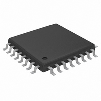
IC CROSSPOINT SWITCH DUAL 32TQFP

MAX9390EHJ+

Manufacturer Part Number
MAX9390EHJ+
Description
IC CROSSPOINT SWITCH DUAL 32TQFP
Manufacturer
Maxim Integrated Products
Datasheet

Specifications of MAX9390EHJ+

Function
Crosspoint Switch
Circuit
2 x 2:2
Voltage Supply Source
Single Supply
Voltage - Supply, Single/dual (±)
3 V ~ 3.6 V
Current - Supply
68mA
Operating Temperature
-40°C ~ 85°C
Mounting Type
Surface Mount
Package / Case
32-TQFP, 32-VQFP
Lead Free Status / RoHS Status
Lead free / RoHS Compliant
The MAX9390/MAX9391 dual 2 x 2 crosspoint switches
perform high-speed, low-power, and low-noise signal
distribution. The MAX9390/MAX9391 multiplex one of two
differential input pairs to either or both low-voltage differ-
ential signaling (LVDS) outputs for each channel.
Independent enable inputs turn on or turn off each differ-
ential output pair.
Four LVCMOS/LVTTL logic inputs (two per channel) con-
trol the internal connections between inputs and outputs.
This flexibility allows for the following configurations: 2 x 2
crosspoint switch, 2:1 mux, 1:2 splitter, or dual repeater.
This makes the MAX9390/MAX9391 ideal for protection
switching in fault-tolerant systems, loopback switching for
diagnostics, fanout buffering for clock/data distribution,
and signal regeneration.
Fail-safe circuitry forces the outputs to a differential low
condition for undriven inputs or when the common-
mode voltage exceeds the specified range. The
MAX9390 provides high-level input fail-safe detection
for LVDS, HSTL, and other GND-referenced differential
inputs. The MAX9391 provides low-level input fail-safe
detection for LVPECL, CML, and other V
differential inputs.
Ultra-low 82ps
(PRBS) jitter ensures reliable communications in high-
speed links that are highly sensitive to timing error,
especially those incorporating clock-and-data recovery,
or serializers and deserializers. The high-speed switch-
ing performance guarantees 1.5GHz operation and less
than 65ps (max) skew between channels.
LVDS inputs and outputs are compatible with the
TIA/EIA-644 LVDS standard. The LVDS outputs drive
100Ω loads. The MAX9390/MAX9391 are offered in a
32-pin TQFP package and operate over the extended
temperature range (-40°C to +85°C).
Also refer to the MAX9392/MAX9393 with flow-through
pinout.
19-2829; Rev 2; 5/07
Functional Diagram and Typical Operating Circuit appear at
end of data sheet.
For pricing, delivery, and ordering information, please contact Maxim/Dallas Direct! at
1-888-629-4642, or visit Maxim’s website at www.maxim-ic.com.
High-Speed Telecom/Datacom Equipment
Central-Office Backplane Clock Distribution
DSLAM
Protection Switching
Fault-Tolerant Systems
(
P-P)
________________________________________________________________ Maxim Integrated Products
(max) pseudorandom bit sequence
General Description
Applications
CC
-referenced
Anything-to-LVDS Dual 2 x 2
♦ 1.5GHz Operation with 250mV Differential Output
♦ 2ps
♦ AC Specifications Guaranteed for 150mV
♦ Signal Inputs Accept Any Differential Signaling
♦ LVDS Outputs for Clock or High-Speed Data
♦ High-Level Input Fail-Safe Detection (MAX9390)
♦ Low-Level Input Fail-Safe Detection (MAX9391)
♦ 3.0V to 3.6V Supply Voltage Range
♦ LVCMOS/LVTTL Logic Inputs Control Signal
+Denotes a lead-free package.
MAX9390EHJ
MAX9390EHJ+
MAX9391EHJ
MAX9391EHJ+
Swing
Differential Input
Standard
Routing
OUTB1
OUTB1
OUTB0
OUTB0
PART
Crosspoint Switches
TOP VIEW
ENB1
ENB0
(RMS)
GND
V
CC
1
2
3
4
7
5
6
8
(max) Random Jitter
+
32
9
-40°C to +85°C
-40°C to +85°C
-40°C to +85°C
-40°C to +85°C
TEMP RANGE
10
31
Ordering Information
30
11
MAX9390
MAX9391
TQFP
29
12
Pin Configurations
28
13
27
14
PIN-
PACKAGE
32 TQFP
32 TQFP
32 TQFP
32 TQFP
26
15
16
25
Features
24 V
23 OUTA0
22
21
20
19
18
17
OUTA0
ENA0
GND
OUTA1
OUTA1
ENA1
CC
CODE
H32-1
H32-1
H32-1
H32-1
PKG
1

Related parts for MAX9390EHJ+

MAX9390EHJ+ Summary of contents

Page 1

... High-Level Input Fail-Safe Detection (MAX9390) ♦ Low-Level Input Fail-Safe Detection (MAX9391) ♦ 3.0V to 3.6V Supply Voltage Range ♦ LVCMOS/LVTTL Logic Inputs Control Signal Routing PART MAX9390EHJ -referenced CC MAX9390EHJ+ MAX9391EHJ MAX9391EHJ+ +Denotes a lead-free package. TOP VIEW ENB1 OUTB1 OUTB1 Applications GND ...

Page 2

Anything-to-LVDS Dual Crosspoint Switches ABSOLUTE MAXIMUM RATINGS V to GND ...........................................................-0.3V to +4.1V CC IN_ _, IN_ _, OUT_ _, OUT_ _, EN_ _, _SEL_ to GND.........................................-0. IN_ _ to IN_ _ ..........................................................................±3V Short-Circuit Duration ...

Page 3

DC ELECTRICAL CHARACTERISTICS (continued) = 100Ω ±1%, EN_ 3.0V to 3.6V -40°C to +85°C, unless otherwise noted. Typical values are at V PARAMETER Output Short-Circuit Current (Either Output Shorted to GND) Output ...

Page 4

Anything-to-LVDS Dual Crosspoint Switches (V = 3.3V 0.2V 1.2V SUPPLY CURRENT vs. TEMPERATURE 3. 3.3V CC ...

Page 5

PIN NAME B1 Output Enable. Drive ENB1 high to enable the B1 LVDS outputs. An internal 435kΩ resistor pulls ENB1 1 ENB1 low when unconnected. B1 LVDS Noninverting Output. Connect a 100Ω termination resistor between OUTB1 and OUTB1 at the ...

Page 6

Anything-to-LVDS Dual Crosspoint Switches PIN NAME A1 Output Enable. Drive ENA1 high to enable the A1 LVDS outputs. An internal 435kΩ resistor pulls ENA1 17 ENA1 low when unconnected. A1 LVDS Inverting Output. Connect a 100Ω termination ...

Page 7

V IN_ IN_ _ t PLH V OUT_ OUT_ _ 80 IN_ _ IN_ ...

Page 8

Anything-to-LVDS Dual Crosspoint Switches 1/4 MAX9390/MAX9391 C L IN_ _ IN_ _ PULSE GENERATOR C L 50Ω = 100Ω ± 1.0pF L Figure 4. Output Active-to-Disable and Disable-to-Active Test Circuit and Timing Diagram ...

Page 9

V OUT_0 OUT_0 t CCS V OUT_1 OUT_1 OUT_ _ OUT_ _ t MEASURED WITH _SEL0 = _SEL1 = HIGH OR LOW CCS (1:2 ...

Page 10

Anything-to-LVDS Dual Crosspoint Switches Table 1. Input/Output Function Table _SEL0 _SEL1 Applications Information Differential Inputs The MAX9390/MAX9391 inputs accept any differential signaling standard within the specified common-mode voltage range. ...

Page 11

Anything-to-LVDS Dual 3.0V TO 3.6V 0.1μF 0.01μ 50Ω INA0 0 100Ω MAX9390 MAX9391 Z = 50Ω INA0 0 INA1 INA1 INB0 INB0 INB1 INB1 ENA0 ENA1 ENB0 ENB1 LVCMOS/LVTTL LOGIC INPUTS ASEL0 ASEL1 ...

Page 12

Anything-to-LVDS Dual Crosspoint Switches Functional Diagram INA0 0 INA0 1 INA1 1 INA1 0 0 OUTB0 OUTB0 ENB0 1 BSEL0 1 OUTB1 OUTB1 ENB1 0 BSEL1 12 ______________________________________________________________________________________ TRANSISTOR COUNT: 1565 PROCESS: BIPOLAR MAX9390 MAX9391 OUTA0 OUTA0 ...

Page 13

For the latest package outline information go to www.maxim-ic.com/packages.) ______________________________________________________________________________________ Anything-to-LVDS Dual Crosspoint Switches PACKAGE OUTLINE, 32L TQFP, 5x5x1.0mm Package Information 1 21-0110 ...

Page 14

... Maxim cannot assume responsibility for use of any circuitry other than circuitry entirely embodied in a Maxim product. No circuit patent licenses are implied. Maxim reserves the right to change the circuitry and specifications without notice at any time. 14 ____________________Maxim Integrated Products, 120 San Gabriel Drive, Sunnyvale, CA 94086 408-737-7600 © 2007 Maxim Integrated Products Package Information (continued) PACKAGE OUTLINE, 32L TQFP, 5x5x1 ...

Related keywords