NB4L858MFAG ON Semiconductor, NB4L858MFAG Datasheet
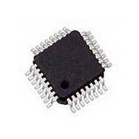
IC CROSSPOINT SWITCH DUAL 32LQFP

NB4L858MFAG

Manufacturer Part Number
NB4L858MFAG
Description
IC CROSSPOINT SWITCH DUAL 32LQFP
Manufacturer
ON Semiconductor
Datasheet

Specifications of NB4L858MFAG

Function
Crosspoint Switch
Circuit
2 x 2:2
Voltage Supply Source
Single Supply
Voltage - Supply, Single/dual (±)
2.3 V ~ 3.6 V
Current - Supply
130mA
Operating Temperature
-40°C ~ 85°C
Mounting Type
Surface Mount
Package / Case
32-LQFP
Lead Free Status / RoHS Status
Lead free / RoHS Compliant

Available stocks

Company
Part Number
Manufacturer
Quantity
Price
Part Number:
NB4L858MFAG
Manufacturer:
ON Semiconductor
Quantity:
40
Part Number:
NB4L858MFAG
Manufacturer:
ON Semiconductor
Quantity:
10 000
NB4L858M
2.5V/3.3V, 3 GHz Dual
Differential Clock/Data 2x2
Crosspoint Switch with
CML Output and Internal
Termination
Description
dual 2 x 2 crosspoint switch with CML outputs that is suitable for
applications such as SDH/SONET DWDM and high speed switching
applications. Design technique minimizes jitter accumulation,
crosstalk, and signal skew which make this device ideal for
loop−through and protection channel switching application. Each
2 x 2 crosspoint switch can fan out and/or multiplex up to 3 Gb/s data
and 3 GHz clock signals.
resistors in a center−tapped configuration (V
LVPECL (Positive ECL) or CML input signal without any external
component. This feature provides transmission line termination
on−chip, at the receiver end, eliminating external components.
Differential 16 mA CML output provides matching internal 50 W
terminations, and 400 mV output swings when externally terminated,
50 W to V
LVCMOS or LVTTL input levels. The device is housed in a low
profile 7 x 7 mm 32−pin LQFP package.
Features
© Semiconductor Components Industries, LLC, 2005
December, 2005 − Rev. 9
The NB4L858M is a high−bandwidth low voltage fully differential
Differential inputs incorporate a pair of internal 50 W termination
The SELECT inputs are single−ended and can be driven with either
Output
Maximum Input Clock Frequency 3 GHz
Maximum Input Data Frequency 3 Gb/s
350 ps Typical Propagation Delay
80 ps Typical Rise and Fall Times
12 ps Channel to Channel Skew
0.5 ps RMS Jitter
5 ps Deterministic Jitter @ 2.5 Gb/s
Operating Range: V
CML Output Level (400 mV Peak−to−Peak Output), Differential
These are Pb−Free Devices
CC
.
CC
= 2.3V to 3.6 V with GND = 0 V
TDx
Pins) and can accept
1
*For additional marking information, refer to
See detailed ordering and shipping information in the package
dimensions section on page 8 of this data sheet.
VTDA0
VTDA1
VTDB0
VTDB1
SELA0
SELA1
SELB0
SELB1
Application Note AND8002/D.
DA0
DA0
DA1
DA1
DB0
DB0
DB1
DB1
Figure 1. Functional Block Diagram
CASE 873A
FA SUFFIX
LQFP−32
A
WL, L
YY, Y
WW, W = Work Week
G
ORDERING INFORMATION
50W
50W
50W
50W
50W
50W
50W
50W
http://onsemi.com
= Assembly Location
= Wafer Lot
= Year
= Pb−Free Package
32
Publication Order Number:
DIAGRAM*
MARKING
1
AWLYYWW
NB4L
858M
0
1
0
1
0
1
0
1
B0
B1
A0
A1
NB4L858M/D
QA0
QA0
QA1
QA1
QB0
QB0
QB1
QB1

Related parts for NB4L858MFAG

NB4L858MFAG Summary of contents

Page 1

NB4L858M 2.5V/3.3V, 3 GHz Dual Differential Clock/Data 2x2 Crosspoint Switch with CML Output and Internal Termination Description The NB4L858M is a high−bandwidth low voltage fully differential dual crosspoint switch with CML outputs that is suitable for applications ...

Page 2

DA0 VTDA0 DA0 SELA1 DA1 VTDA1 DA1 SELA0 Table 1. TRUTH TABLE SELA0/SELB0 SELA1/SELB1 NB4L858M GND V QA0 QA0 V QA1 QA1 ...

Page 3

Table 2. PIN DESCRIPTION Pin Name 1 DB1 LVPECL, CML Input 2 VTDB1 3 DB1 LVPECL, CML Input 4 SELB0 LVTTL / LVCMOS 5 DB0 LVPECL, CML Input 6 VTDB0 7 DB0 LVPECL, CML Input 8 SELB1 LVTTL / LVCMOS ...

Page 4

Table 3. Table 3. ATTRIBUTES ESD Protection Moisture Sensitivity (Note 1) Flammability Rating Transistor Count Meets or exceeds JEDEC Spec EIA/JESD78 IC Latchup Test 1. For additional information, see Application Note AND8003/D. Table 4. MAXIMUM RATINGS Symbol Parameter V Positive ...

Page 5

Table 5. DC CHARACTERISTICS, CLOCK INPUTS, CML OUTPUTS Symbol I Power Supply Current CC V CML Differential Output Swing (Note 3) No Load outdiff Loaded Output HIGH Voltage (No Load Output LOW ...

Page 6

Table 6. AC CHARACTERISTICS V CC Symbol Characteristic V Output Voltage Amplitude (@ V OUTPP (See Figure 2) f Maximum Operating Data Rate DATA t , Propagation Delay to Output Differential PLH t D/D to Q/Q PHL t SELyx to ...

Page 7

Q Driver Device Q Figure 4. Typical Termination for Output Driver and Device Evaluation TDX GND Input Figure 5. CML Input and Output Structure NB4L858M Dx V ...

Page 8

... ORDERING INFORMATION Device NB4L858MFAG NB4L858MFAR2G †For information on tape and reel specifications, including part orientation and tape sizes, please refer to our Tape and Reel Packaging Specifications Brochure, BRD8011/D. NB4L858M 320 mV MIN (Q − 500 mV MAX (Q − Figure 6. CML Output Levels Package LQFP−32 (Pb− ...

Page 9

−T− DETAIL −Z− −AB− SEATING −AC− PLANE 0.10 (0.004 DETAIL AD NB4L858M PACKAGE DIMENSIONS LQFP FA ...

Page 10

... Fax: 303−675−2176 or 800−344−3867 Toll Free USA/Canada Email: orderlit@onsemi.com NB4L858M N. American Technical Support: 800−282−9855 Toll Free USA/Canada Japan: ON Semiconductor, Japan Customer Focus Center 2−9−1 Kamimeguro, Meguro−ku, Tokyo, Japan 153−0051 Phone: 81−3−5773−3850 http://onsemi.com 10 ON Semiconductor Website: http://onsemi ...

Related keywords