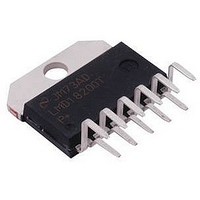
LM3886T National Semiconductor, LM3886T Datasheet - Page 19

LM3886T
Manufacturer Part Number
LM3886T
Description
92F298
Manufacturer
National Semiconductor
Datasheet
1.LM3886TNOPB.pdf
(24 pages)
Specifications of LM3886T
Amplifier Class
AB
No. Of Channels
1
Output Power
68W
Supply Voltage Range
20V To 84V
Load Impedance
4ohm
Operating Temperature Range
-20°C To +85°C
Amplifier Case Style
TO-220
Rohs Compliant
No
Available stocks
Company
Part Number
Manufacturer
Quantity
Price
Part Number:
LM3886T
Manufacturer:
NS/国半
Quantity:
20 000
Part Number:
LM3886TF
Manufacturer:
CN/如韵
Quantity:
20 000
Company:
Part Number:
LM3886TF/NOPB
Manufacturer:
AVX
Quantity:
40 000
Part Number:
LM3886TF/NOPB
Manufacturer:
TI/德州仪器
Quantity:
20 000
Application Information
Typical signal-to-noise figures are listed for an A-weighted
filter which is commonly used in the measurement of noise.
The shape of all weighting filters is similar, with the peak of
the curve usually occurring in the 3 kHz–7 kHz region as
shown below.
SUPPLY BYPASSING
The LM3886 has excellent power supply rejection and does
not require a regulated supply. However, to eliminate pos-
sible oscillations all op amps and power op amps should
have their supply leads bypassed with low-inductance ca-
pacitors having short leads and located close to the package
terminals. Inadequate power supply bypassing will manifest
itself by a low frequency oscillation known as “motorboating”
or by high frequency instabilities. These instabilities can be
eliminated through multiple bypassing utilizing a large tanta-
lum or electrolytic capacitor (10 µF or larger) which is used to
absorb low frequency variations and a small ceramic capaci-
tor (0.1 µF) to prevent any high frequency feedback through
the power supply lines.
If adequate bypassing is not provided the current in the
supply leads which is a rectified component of the load
current may be fed back into internal circuitry. This signal
causes low distortion at high frequencies requiring that the
supplies be bypassed at the package terminals with an
electrolytic capacitor of 470 µF or more.
LEAD INDUCTANCE
Power op amps are sensitive to inductance in the output
lead, particularly with heavy capacitive loading. Feedback to
the input should be taken directly from the output terminal,
minimizing common inductance with the load.
Lead inductance can also cause voltage surges on the sup-
plies. With long leads to the power supply, energy is stored in
the lead inductance when the output is shorted. This energy
can be dumped back into the supply bypass capacitors when
the short is removed. The magnitude of this transient is
reduced by increasing the size of the bypass capacitor near
the IC. With at least a 20 µF local bypass, these voltage
surges are important only if the lead length exceeds a couple
feet (
and ground leads minimizes the effect.
LAYOUT, GROUND LOOPS AND STABILITY
The LM3886 is designed to be stable when operated at a
closed-loop gain of 10 or greater, but as with any other
high-current amplifier, the LM3886 can be made to oscillate
under certain conditions. These usually involve printed cir-
cuit board layout or output/input coupling.
When designing a layout, it is important to return the load
ground, the output compensation ground, and the low level
>
1 µH lead inductance). Twisting together the supply
01183314
(Continued)
19
(feedback and input) grounds to the circuit board common
ground point through separate paths. Otherwise, large cur-
rents flowing along a ground conductor will generate volt-
ages on the conductor which can effectively act as signals at
the input, resulting in high frequency oscillation or excessive
distortion. It is advisable to keep the output compensation
components and the 0.1 µF supply decoupling capacitors as
close as possible to the LM3886 to reduce the effects of PCB
trace resistance and inductance. For the same reason, the
ground return paths should be as short as possible.
In general, with fast, high-current circuitry, all sorts of prob-
lems can arise from improper grounding which again can be
avoided by returning all grounds separately to a common
point. Without isolating the ground signals and returning the
grounds to a common point, ground loops may occur.
“Ground Loop” is the term used to describe situations occur-
ring in ground systems where a difference in potential exists
between two ground points. Ideally a ground is a ground, but
unfortunately, in order for this to be true, ground conductors
with zero resistance are necessary. Since real world ground
leads possess finite resistance, currents running through
them will cause finite voltage drops to exist. If two ground
return lines tie into the same path at different points there will
be a voltage drop between them. The first figure below
shows a common ground example where the positive input
ground and the load ground are returned to the supply
ground point via the same wire. The addition of the finite wire
resistance, R
two points as shown below.
The load current I
I
Therefore the voltage appearing at the non-inverting input is
effectively positive feedback and the circuit may oscillate. If
there were only one device to worry about then the values of
R
however, several devices normally comprise a total system.
Any ground return of a separate device, whose output is in
I
, thus V
1
and R
1
2
will follow the output voltage directly, i.e. in phase.
would probably be small enough to be ignored;
2
, results in a voltage difference between the
L
will be much larger than input bias current
01183315
www.national.com


