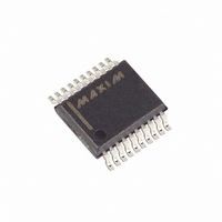
MAX4589CAP+ Maxim Integrated Products, MAX4589CAP+ Datasheet - Page 14

MAX4589CAP+
Manufacturer Part Number
MAX4589CAP+
Description
IC RF/VIDEO MUX DUAL 2CH 20-SSOP
Manufacturer
Maxim Integrated Products
Series
4000r
Datasheet
1.MAX4589EWP.pdf
(20 pages)
Specifications of MAX4589CAP+
Function
Video Multiplexer
Circuit
2 x 2:1
On-state Resistance
60 Ohm
Voltage Supply Source
Single, Dual Supply
Voltage - Supply, Single/dual (±)
2.7 V ~ 12 V, ± 2.7 V ~ 6 V
Operating Temperature
0°C ~ 70°C
Mounting Type
Surface Mount
Package / Case
20-SSOP
Lead Free Status / RoHS Status
Lead free / RoHS Compliant
The MAX4589 construction is typical of many CMOS
analog switches. It has four supply pins: V+, V-, V
GND. V+ and V- are used to drive the internal CMOS
switches and set the limits of the analog voltage on any
switch. Reverse ESD-protection diodes are internally
connected between each analog signal pin and both
V+ and V-. If the voltage on any pin exceeds V+ or V-,
one of these diodes conducts. During normal operation
these reverse-biased ESD diodes leak, forming the only
current drawn from V- and V+.
Virtually all the analog leakage current is through the
ESD diodes. Although the ESD diodes on a given sig-
nal pin are identical, and therefore fairly well balanced,
they are reverse-biased differently. Each is biased by
either V+ or V- and the analog signal. This means their
leakages vary as the signal varies. The difference in the
two diode leakages from the signal path to the V+ and
V- pins constitutes the analog signal-path leakage cur-
rent. All analog leakage current flows to the supply ter-
minals, not to the other switch terminal. This explains
how both sides of a given switch can show leakage
currents of either the same or opposite polarity.
There is no connection between the analog signal
paths and GND. The analog signal paths consist of an
Low-Voltage, High-Isolation,
Dual 2-Channel RF/Video Multiplexer
Figure 8. T-Switch Construction
14
__________Applications Information
______________________________________________________________________________________
Power-Supply Considerations
NO_
GND
V+
V
A_
V-
L
A1
CONTROL
LOGIC
Overview
L
, and
A2
N-channel and P-channel MOSFET with their sources
and drains paralleled and their gates driven out of
phase to V+ and V- by the logic-level translators.
V
translators, and set the input logic thresholds. The
logic-level translators convert the logic levels to
switched V+ and V- signals to drive the gates of the
analog switches. Therefore, the gate-to-source and
gate-to-drain impedances are the only connection
between the logic supplies and the analog supplies.
The MAX4589 operates with bipolar supplies between
±2.7V and ±6V. The V+ and V- supplies are not
required to be symmetrical, but their sum cannot
exceed the absolute maximum rating of 13.0V. Do not
connect the MAX4589 V+ pin to +3V and connect the
logic-level input pins to TTL logic-level signals. This
exceeds the absolute maximum ratings, and may
cause damage to the part and/or external circuits.
CAUTION: The absolute maximum V+ to V- differen-
tial voltage is 13.0V. Typical “±6-Volt” or “12-Volt”
supplies with ±10% tolerances can be as high as
13.2V. This voltage can damage the MAX4589. Even
±5% tolerance supplies may have overshoot or
noise spikes that exceed 13.0V.
L
N1
P1
and GND power the internal logic and logic-level
N3
N2
P2
Bipolar-Supply Operation
COM_


