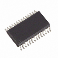
MAX4550CWI+ Maxim Integrated Products, MAX4550CWI+ Datasheet - Page 14

MAX4550CWI+
Manufacturer Part Number
MAX4550CWI+
Description
IC CROSSPOINT SWITCH DUAL 28SOIC
Manufacturer
Maxim Integrated Products
Datasheet
1.MAX4570EAI.pdf
(16 pages)
Specifications of MAX4550CWI+
Function
Audio/Video Crosspoint Switch
Circuit
2 x 4:2
On-state Resistance
100 Ohm
Voltage Supply Source
Single, Dual Supply
Voltage - Supply, Single/dual (±)
2.7 V ~ 5.5 V, ±2.7 V ~ 5.5 V
Current - Supply
7µA
Operating Temperature
0°C ~ 70°C
Mounting Type
Surface Mount
Package / Case
28-SOIC (0.300", 7.50mm Width)
Lead Free Status / RoHS Status
Lead free / RoHS Compliant
To program several MAX4570s individually using a sin-
gle processor, connect DIN of each MAX4570 together
and control CS on each MAX4570 separately. To select
a particular device, drive the corresponding CS low,
clock in the 16-bit command, then drive CS high and
execute the command. Typically, only one MAX4570 is
addressed at a time.
To improve off-isolation, connect the SA or SB input to
ground either directly (DC ground) or through capaci-
tors (AC ground). Closing SA or SB effectively grounds
the unused outputs.
Use the internal bias-resistor networks to give the
switch outputs a DC bias when the switch terminals are
AC coupled. Programming of the switches that connect
the bias resistors to the outputs is accomplished via bit
C5 of the command byte. Connect the BIASH and
BIASL inputs to DC levels (for example, V+ and GND),
and activate the switch connecting the appropriate out-
put. This applies a voltage midway between V
and V
Functional Diagram ).
Serially Controlled, Dual 4x2, Clickless
Audio/Video Analog Crosspoint Switches
Table 6. 3-Wire Serial-Interface Data Format
X = Don’t care
14
MSB
C7
X
______________________________________________________________________________________
BIASL
C6
X
to the output (refer to Tables 1, 4, and the
Using the Internal Bias Resistors
BIAS
C5
AUX
C4
Addressable Serial Interface
Improving Off-Isolation
COMMAND BYTE
COM2B
C3
COM1B
C2
BIASH
COM2A
C1
COM1A
The four auxiliary outputs provide a way to control
external circuitry, such as LEDs or other DC loads,
through the serial interface. Program these outputs via
bit C4 of the command byte. Each output is capable of
sourcing 1mA or sinking 12mA. They are programmed
through the command byte and data byte (refer to
Tables 1, 3, and the Functional Diagram ).
Audible switching transients (“clicks”) are eliminated in
this mode of operation. When an output is configured
as “clickless,” the gate signal of the switches connect-
ed to that output are controlled with slow-moving volt-
ages. As a result, the output slew rates are significantly
reduced. Program clickless operation via bit C5 of the
command byte (refer to Tables 1, 4, and the Functional
Diagram ). Each operating switch may draw as much as
2mA during transition.
The MAX4550/MAX4570 feature a preset power-up
state. Upon power-up, COM1A and COM2A are con-
nected to SA, COM1B and COM2B are connected to
SB, all outputs are set to clickless mode, all bias-resis-
tor networks are disconnected from the outputs, and all
auxiliary outputs are low. All other switches are open.
C0
D7
D7
D6
D6
Using the Auxiliary Outputs
D5
D5
DATA BYTE
D4
D4
Clickless Switching
D3
D3
Power-Up State
D2
D2
D1
D1
LSB
D0
D0


