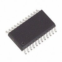
MAX395CWG+ Maxim Integrated Products, MAX395CWG+ Datasheet - Page 14

MAX395CWG+
Manufacturer Part Number
MAX395CWG+
Description
IC SWITCH OCTAL SPST 24SOIC
Manufacturer
Maxim Integrated Products
Datasheet
1.MAX395EWG.pdf
(16 pages)
Specifications of MAX395CWG+
Function
Switch
Circuit
8 x SPST - NO
On-state Resistance
175 Ohm
Voltage Supply Source
Single, Dual Supply
Voltage - Supply, Single/dual (±)
2.7 V ~ 16 V, ±2.7 V ~ 8 V
Current - Supply
7µA
Operating Temperature
0°C ~ 70°C
Mounting Type
Surface Mount
Package / Case
24-SOIC (0.300", 7.50mm Width)
Lead Free Status / RoHS Status
Lead free / RoHS Compliant
SCLK, each switch sequences one differential channel
at a time, starting with channel 7/0. After the first eight
bits have been sent, subsequent channel sequencing
can occur by repeating this sequence or, even faster,
by sending only one DIN high pulse and one CS low
pulse for each four clock pulses.
To use the MAX395 as a quad, single-pole/double-
throw (SPDT) switch, connect COM0 to NO1, COM2 to
NO3, COM4 to NO5, and COM6 to NO7, forming the
four “common” pins. Program these four switches with
pairs of instructions, as shown in Table 2.
Serially Controlled, Low-Voltage,
8-Channel SPST Switch
Figure 6. Addressable Serial Interface
Figure 7. Differential Multiplexer Input Control
14
SCLK
DIN
______________________________________________________________________________________
SCLK
CS1
CS3
CS2
DIN
SW4
D4
CS
SCLK
DIN
MAX395
FOUR CLOCK
PULSES
SPDT Switches
SW0
D0
CS
SCLK
DIN
MAX395
RESET is the internal reset pin. It is usually connected
to a logic signal or V+. Drive RESET low to open all
switches and set the contents of the internal shift regis-
ter to zero simultaneously. When RESET is high, the
part functions normally and DOUT is sourced from V+.
RESET must not be driven beyond V+ or GND.
The MAX395 construction is typical of most CMOS ana-
log switches. It has three supply pins: V+, V-, and
GND. V+ and V- are used to drive the internal CMOS
switches and to set the limits of the analog voltage on
any switch. Reverse ESD-protection diodes are inter-
nally connected between each analog signal pin and
both V+ and V-. If any analog signal exceeds V+ or V-,
one of these diodes will conduct. During normal opera-
tion, these (and other) reverse-biased ESD diodes leak,
forming the only current drawn from V+ or V-.
Virtually all the analog leakage current is through the
ESD diodes. Although the ESD diodes on a given sig-
nal pin are identical, and therefore fairly well balanced,
they are reverse biased differently. Each is biased by
either V+ or V- and the analog signal. This means their
leakages vary as the signal varies. The difference in the
two diode leakages to the V+ and V- pins constitutes
the analog signal-path leakage current. All analog leak-
Power-Supply Considerations
CS
SCLK
DIN
MAX395
Reset Function
TO OTHER
SERIAL
DEVICES
Overview


