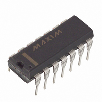
DG303ACJ+ Maxim Integrated Products, DG303ACJ+ Datasheet - Page 3

DG303ACJ+
Manufacturer Part Number
DG303ACJ+
Description
IC SWITCH DUAL SPDT 14DIP
Manufacturer
Maxim Integrated Products
Type
Analog Switchr
Datasheet
1.DG303ACWE.pdf
(11 pages)
Specifications of DG303ACJ+
Function
Switch
Circuit
2 x SPDT
On-state Resistance
50 Ohm
Voltage Supply Source
Dual Supply
Voltage - Supply, Single/dual (±)
±5 V ~ 18 V
Operating Temperature
0°C ~ 70°C
Mounting Type
Through Hole
Package / Case
14-DIP (0.300", 7.62mm)
Number Of Switches
Single
Switch Configuration
SPDT
On Resistance (max)
50 Ohms
On Time (max)
300 ns
Off Time (max)
250 ns
Off Isolation (typ)
62 dB
Supply Voltage (max)
18 V
Supply Voltage (min)
5 V
Supply Current
0.23 mA
Maximum Power Dissipation
470 mW
Maximum Operating Temperature
+ 70 C
Mounting Style
Through Hole
Minimum Operating Temperature
0 C
Off State Leakage Current (max)
0.1 nA
Package
14PDIP N
Maximum On Resistance
50@±15V Ohm
Maximum High Level Output Current
30 mA
Number Of Channels Per Chip
2
Maximum Turn-off Time
250@±15V ns
Maximum Turn-on Time
300@±15V ns
Switch Architecture
SPDT
Power Supply Type
Single|Dual
Lead Free Status / RoHS Status
Lead free / RoHS Compliant
ELECTRICAL CHARACTERISTICS (Over Temperature)
(V+ = +15V, V- = -15V, GND = 0V, T
ELECTRICAL CHARACTERISTICS (continued)
(V+ = +15V, V- = -15V, GND = 0V, T
Positive Supply
Current
Negative Supply
Current
Positive Supply
Current
Negative Supply
Current
Analog Signal Range
Drain-Source
ON-Resistance
Source OFF-
Leakage Current
Drain OFF-
Leakage Current
Drain ON-
Leakage Current
Input Current/
Voltage High
Input Current/
Voltage Low
Positive Supply
Current
Negative Supply
Current
Positive Supply
Current
Negative Supply
Current
Turn-ON Time
Turn-OFF Time
PARAMETER
PARAMETER
_______________________________________________________________________________________
TTL Compatible CMOS Analog Switches
SYMBOL
SYMBOL
V
R
I
I
ANALOG
I
S(OFF)
D(OFF)
DS(ON)
D(ON)
t
I
I
t
OFF
INH
INL
I+
I+
I+
I+
ON
I-
I-
I-
I-
A
A
= +25°C, unless otherwise noted.)
= Over Temperature Range, unless otherwise noted.)
I
V
V
V
V
(all others = 0)
V
See Switching Time Test Circuit
V
(all others = 0)
V
V
V
S
IN
IN
IN
IN
IN
IN
IN
IN
IN
= -10mA, V
= 4V (one input)
= 0.8V (all inputs)
= 5.0V
= 15V
= 0V
= 4V (one input)
= 0.8V (all inputs)
= 0.8V
= 0.8V
or
TEST CONDITIONS
TEST CONDITIONS
I
I
V
V
V
V
V
V
IN
S
S
S
S
S
S
D
D
= -10mA, V
= -10mA, V
= 0.8V or 4.0V
= 14V, V
= -14V, V
= -14V, V
= 14V, V
= V
= V
S
S
= 14V
= -14V
D
D
D
D
D
D
= -14V
= -14V
= 14V
= 14V
= 10V
= -10V
(Note 2)
(Note 2)
-100
-100
-200
-100
-100
MIN
MIN
DG300A–DG303AA
DG300A–DG303AA
-10
-10
-15
-1
-1
DG300–DG303A
DG300–DG303A
(Note 3)
(Note 3)
-0.001
-0.001
0.001
TYP
TYP
0.23
MAX
MAX
+15
100
100
200
100
500
450
0.5
10
75
75
1
1
(Note 2)
(Note 2)
DG300A–DG303AB/C
DG300A–DG303AB/C
-100
-100
-200
-200
-200
MIN
MIN
-10
-10
DG300–DG303B/C
-15
-10
-10
DG300–DG303B/C
(Note 3)
(Note 3)
-0.001
-0.001
0.001
TYP
0.23
TYP
MAX
MAX
+15
100
100
200
200
0.5
10
75
75
10
1
UNITS
UNITS
mA
mA
mA
µA
µA
µA
nA
nA
nA
µA
µA
µA
µA
ns
ns
Ω
V
3


