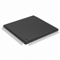
MAX9675ECQ+T Maxim Integrated Products, MAX9675ECQ+T Datasheet - Page 14

MAX9675ECQ+T
Manufacturer Part Number
MAX9675ECQ+T
Description
IC CROSSPOINT SWIT 16X16 100TQFP
Manufacturer
Maxim Integrated Products
Datasheet
1.MAX9675ECQT.pdf
(27 pages)
Specifications of MAX9675ECQ+T
Function
Crosspoint Switch
Circuit
1 x 16:16
Voltage Supply Source
Single Supply
Voltage - Supply, Single/dual (±)
2.7 V ~ 5.5 V
Operating Temperature
-40°C ~ 85°C
Mounting Type
Surface Mount
Package / Case
100-TQFP Exposed Pad
Lead Free Status / RoHS Status
Lead free / RoHS Compliant
110MHz, 16 x 16 Video Crosspoint
Switch with Programmable Gain
14
2, 4, 6, 8, 10, 12, 14, 16,
1, 3, 5, 7, 9, 11, 13, 15,
45, 46, 82, 83, 84, 91,
25, 47, 51, 55, 59, 63,
48, 50, 52, 54, 56, 58,
60, 62, 64, 66, 68, 70,
49, 53, 57, 61, 65, 69,
26, 27, 38–44, 76, 77,
______________________________________________________________________________________
85–89, 99, 100
17, 19, 21, 23
18, 20, 22, 24
67, 71, 75, 81
72, 74, 78, 80
90, 92, 94, 96
93, 95, 97
73, 79, 98
PIN
28
29
30
31
32
33
34
35
36
37
OUT15–OUT0
IN4–IN15
UPDATE
IN0–IN3
RESET
NAME
AGND
A3–A0
DGND
MODE
DOUT
AOUT
SCLK
V
N.C.
V
DIN
V
CE
CC
DD
EE
Buffered Analog Inputs
Analog Ground
Address Programming Inputs. Connect to DGND or V
Individual Output Address Mode (see Table 3).
Positive Analog Supply. Bypass each pin with a 0.1µF capacitor to AGND. Connect
a single 10µF capacitor from one V
No Connection. Not internally connected. Connect to AGND.
Serial-Data Output. In Complete Matrix Mode, data is clocked through the 96-bit
Matrix Control shift register. In Individual Output Address Mode, data at DIN
passes directly to DOUT.
Digital Ground
Address Recognition Output. AOUT drives low after successful chip address
recognition.
Serial-Clock Input
Clock Enable Input. Drive low to enable the serial data interface.
Serial Interface Mode Select Input. Drive high for Complete Matrix Mode (Mode 1)
or drive low for Individual Output Address Mode (Mode 0).
Asynchronous Reset Input/Output. Drive RESET low to initiate hardware reset. All
matrix settings are set to power up defaults and all analog outputs are disabled.
Additional power-on-reset delay may be set by connecting a small capacitor from
RESET to DGND.
Update Input. Drive UPDATE low to transfer data from mode registers to the switch
matrix.
Serial-Data Input. Data is clocked in on the falling edge of SCLK.
Digital Logic Supply. Bypass V
Buffered Analog Outputs. Gain is individually programmable for A
= +2V/V through the serial interface. Outputs may be individually disabled (high
impedance). On power-up, or assertion of RESET, all outputs are disabled.
Negative Analog Supply. Bypass each pin with a 0.1µF capacitor to AGND.
Connect a single 10µF capacitor from one V
Buffered Analog Inputs
DD
with a 0.1µF capacitor to DGND.
CC
FUNCTION
pin to AGND.
EE
pin to AGND.
DD
Pin Description
to select the address for
V
= +1V/V or A
V


