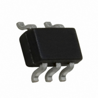
FSAT66P5X Fairchild Semiconductor, FSAT66P5X Datasheet - Page 3

FSAT66P5X
Manufacturer Part Number
FSAT66P5X
Description
IC SWITCH SPST SC70-5
Manufacturer
Fairchild Semiconductor
Datasheet
1.FSAT66P5X.pdf
(10 pages)
Specifications of FSAT66P5X
Function
Switch
Circuit
1 x SPST- NO
On-state Resistance
15 Ohm
Voltage Supply Source
Single Supply
Voltage - Supply, Single/dual (±)
1.65 V ~ 5.5 V
Current - Supply
10µA
Operating Temperature
-40°C ~ 85°C
Mounting Type
Surface Mount
Package / Case
6-TSSOP (5 lead), SC-88A, SOT-353
Lead Free Status / RoHS Status
Lead free / RoHS Compliant
Symbol
V
V
I
I
R
R
I
IN
OFF
CC
Absolute Maximum Ratings
DC Electrical Characteristics
Note 4: All typical values are at the specified V
Note 5: Measured by the voltage drop between A and B pins at the indicated current through the switch. On Resistance is determined by the lower of the
voltages on the two (A or B) pins.
Note 6: Parameter is characterized but not tested in production.
Note 7: Flatness is defined as the difference between the minimum and maximum value of On Resistance over the specified range of conditions.
IH
IL
ON
flat
Supply Voltage (V
DC Switch Voltage (V
DC Input Voltage (V
DC Input Diode Current
DC Output (I
DC V
Storage Temperature Range (T
Junction Lead Temperature
Junction Lead Temperature (T
Power Dissipation (P
@ (I
under Bias (T
(Soldering, 10 Seconds)
SC70-5
MicroPak-6
CC
IK
HIGH Level Input
Voltage
LOW Level Input
Voltage
Control Input
Leakage Current
OFF Leakage Current
Switch On Resistance
(Note 5)
On Resistance Flatness
(Note 5)(Note 6)
(Note 7)
Quiescent Supply
Current
) V
or Ground Current (I
IN
Parameter
OUT
0V
J
) Sink Current
)
CC
IN
)
D
S
) (Note 2)
) @ 85 C
)
1.65 to 3.6 (0.25 V
1.65 to 3.6
1.65 to 5.5
1.65 to 5.5
CC
4.5 to 5.5
4.5 to 5.5
0 to 5.5
L
STG
)
V
1.65
/I
(V)
4.5
3.0
2.3
5.0
3.3
2.5
1.8
GND
CC
)
CC
)
, and T
0.5V to V
Min
2.0
65 C to 150 C
A
T
CC
0.5V to 7.0V
0.5V to 7.0V
A
(Note 1)
25 C.
40 C to 85 C
(Note 4)
CC
0.75)
150 mW
200 mW
10.0
13.0
25.0
Typ
128 mA
100 mA
3.0
5.0
7.0
4.0
5.0
7.0
50 mA
150 C
260 C
0.5V
0.165 V
3
Max
12.0
15.0
20.0
12.0
30.0
28.0
60.0
10.0
0.8
10.0
7.0
9.0
1.0
Recommended Operating
Conditions
Note 1: The “Absolute Maximum Ratings” are those values beyond which
the safety of the device cannot be guaranteed. The device should not be
operated at these limits. The parametric values defined in the Electrical
Characteristics tables are not guaranteed at the absolute maximum ratings.
The “Recommended Operating Conditions” table will define the conditions
for actual device operation.
Note 2: The input and output negative voltage ratings may be exceeded if
the input and output diode current ratings are observed.
Note 3: Unused inputs must be held HIGH or LOW. They may not float.
Power Supply Voltage (V
Control Input Voltage (V
Switch Input Voltage (V
Switch Output Voltage (V
Input Rise and Fall Time (t
Operating Temperature (T
Thermal Resistance (
CC
Control Input V
Control Input V
Switch I/O
SC70-5
MicroPak-6
Min
T
A
12.0
28.0
Typ
125
6.0
CC
CC
25 C
(Note 3)
2.3V to 3.6V
4.5V to 5.5V
JA
Max
IN
IN
)
CC
)
OUT
)
A
r
, t
)
)
f
)
)
Units
V
V
A
A
A
0
0
V
V
V
V
V
V
V
V
V
I
I
I
I
V
I
A
A
A
A
OUT
IN
IN
IN
IN
IN
IN
IN
IN
IN
IN
www.fairchildsemi.com
V
A, B
0 ns/V to 10 ns/V
IN
30 mA, 0
24 mA, 0
8 mA, 0
4 mA, 0
0V, I
2.4V, I
4.5V, I
0V, I
3V, I
0V, I
2.3V, I
0V, I
1.65V, I
V
0 ns/V to 5 ns/V
0
CC
Conditions
40 C to 85 C
1.65V to 5.5V
5.5V
0 ns/V to DC
IN
IN
IN
IN
IN
V
or GND
425 C/Watt
325 C/Watt
CC
IN
IN
IN
0V to 5.5V
IN
0V to V
0V to V
30 mA
24 mA
24 mA
8 mA
4 mA
V
V
15 mA
30 mA
8 mA
V
V
Bn
Bn
4 mA
Bn
Bn
CC
CC
V
V
V
V
CC
CC
CC
CC


