ADG725BSU-REEL Analog Devices Inc, ADG725BSU-REEL Datasheet
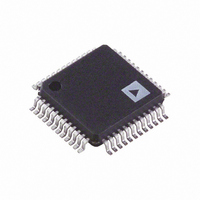
IC MULTIPLEXER DUAL 16X1 48TQFP

ADG725BSU-REEL

Manufacturer Part Number
ADG725BSU-REEL
Description
IC MULTIPLEXER DUAL 16X1 48TQFP
Manufacturer
Analog Devices Inc
Datasheet

Specifications of ADG725BSU-REEL

Rohs Status
RoHS non-compliant
Function
Multiplexer
Circuit
2 x 16:1
On-state Resistance
5.5 Ohm
Voltage Supply Source
Single, Dual Supply
Voltage - Supply, Single/dual (±)
1.8 V ~ 5.5 V, ±2.5 V
Current - Supply
10µA
Operating Temperature
-40°C ~ 85°C
Mounting Type
Surface Mount
Package / Case
48-TQFP, 48-VQFP
a
GENERAL DESCRIPTION
The ADG731/ADG725 are monolithic, CMOS, 32-channel/
dual 16-channel analog multiplexers with a serially controlled
3-wire interface. The ADG731 switches one of 32 inputs
(S1–S32) to a common output, D. The ADG725 can be config-
ured as a dual mux switching one of 16 inputs to one output, or a
differential mux switching one of 16 inputs to a differential output.
These mulitplexers utilize a 3-wire serial interface that is com-
patible with SPI
interface standards. On power-up, the Internal Shift Register
contains all zeros and all switches are in the OFF state.
These multiplexers are designed on an enhanced submicron
process that provides low power dissipation yet gives high switch-
ing speed with very low on resistance and leakage currents.
They operate from a single supply of 1.8 V to 5.5 V or a
± 2.5 V dual supply, making them ideally suited to a variety of
applications. On resistance is in the region of a few ohms, is
closely matched between switches, and is very flat over the full
signal range.
REV. A
Information furnished by Analog Devices is believed to be accurate and
reliable. However, no responsibility is assumed by Analog Devices for its
use, nor for any infringements of patents or other rights of third parties that
may result from its use. No license is granted by implication or otherwise
under any patent or patent rights of Analog Devices. Trademarks and
registered trademarks are the property of their respective companies.
FEATURES
3-Wire SPI Compatible Serial Interface
1.8 V to 5.5 V Single Supply
4
0.5
7 mm x 7 mm 48-Lead Chip Scale Package (LFCSP)
Rail-to-Rail Operation
Power-On Reset
42 ns Switching Times
Single 32-to-1 Channel Multiplexer
Dual/Differential 16-to-1 Channel Multiplexer
TTL/CMOS Compatible Inputs
For Functionally Equivalent Devices with Parallel
APPLICATIONS
Optical Applications
Data Acquisition Systems
Communication Systems
Relay Replacement
Audio and Video Switching
Battery-Powered Systems
Medical Instrumentation
Automatic Test Equipment
2.5 V Dual-Supply Operation
or 48-Lead TQFP Package
Interface, See ADG726/ADG732
On Resistance
On Resistance Flatness
®
, QSPI
, MICROWIRE
, and some DSP
1.8 V to 5.5 V, 2.5 V, Analog Multiplexers
16-/32-Channel, Serially Controlled 4
These parts can operate equally well as either multiplexers or
demultiplexers and have an input signal range that extends to the
supplies. In the OFF condition, signal levels up to the supplies
are blocked. All channels exhibit break-before-make switching
action, preventing momentary shorting when switching channels.
The ADG731 and ADG725 are serially controlled 32-channel,
and dual/differential 16-channel multiplexers, respectively. They
are available in either a 48-lead LFCSP or TQFP package.
PRODUCT HIGHLIGHTS
1.
2.
3.
4.
5.
One Technology Way, P.O. Box 9106, Norwood, MA 02062-9106, U.S.A.
Tel: 781/329-4700
Fax: 781/326-8703
3-Wire Serial Interface.
1.8 V to 5.5 V Single-Supply or ± 2.5 V Dual-Supply
Operation. These parts are specified and guaranteed
with 5 V ± 10%, 3 V ± 10% single-supply,
and ± 2.5 V ± 10% dual-supply rails.
On Resistance of 4 W.
Guaranteed Break-Before-Make Switching Action.
7 mm ¥ 7 mm 48-Lead Chip Scale Package (LFCSP) or
48-Lead TQFP Package.
S32
S1
SCLK DIN SYNC
INPUT SHIFT
FUNCTIONAL BLOCK DIAGRAM
ADG731
REGISTER
© 2003 Analog Devices, Inc. All rights reserved.
ADG725/ADG731
D
S16A
S16B
S1A
S1B
SCLK DIN SYNC
INPUT SHIFT
ADG725
REGISTER
www.analog.com
DA
DB

Related parts for ADG725BSU-REEL

ADG725BSU-REEL Summary of contents

Page 1

FEATURES 3-Wire SPI Compatible Serial Interface 1 5.5 V Single Supply 2.5 V Dual-Supply Operation 4 On Resistance 0.5 On Resistance Flatness 48-Lead Chip Scale Package (LFCSP) or 48-Lead TQFP Package Rail-to-Rail ...

Page 2

ADG725/ADG731–SPECIFICATIONS Parameter ANALOG SWITCH Analog Signal Range On Resistance ( Resistance Match between Channels (∆ Resistance Flatness (R ) FLAT(ON) LEAKAGE CURRENTS Source OFF Leakage I (OFF) S Drain OFF Leakage I (OFF) D ...

Page 3

SPECIFICATIONS (V DD Parameter ANALOG SWITCH Analog Signal Range On Resistance ( Resistance Match between Channels (∆ Resistance Flatness (R ) FLAT(ON) LEAKAGE CURRENTS Source OFF Leakage I (OFF) S Drain OFF Leakage ...

Page 4

ADG725/ADG731 DUAL-SUPPLY SPECIFICATIONS Parameter ANALOG SWITCH Analog Signal Range On Resistance ( Resistance Match Between Channels (∆ Resistance Flatness (R ) FLAT(ON) LEAKAGE CURRENTS Source OFF Leakage I (OFF) S Drain OFF Leakage I ...

Page 5

TIMING CHARACTERISTICS Parameter Limit MIN MAX f 30 SCLK 4 NOTES 1 See ...

Page 6

... Operating Temperature Range Industrial (B Version –40°C to +85°C Model Temperature Range o ADG725BCP – +85 o ADG725BCP-REEL – +85 o ADG725BCP-REEL7 – +85 o ADG725BSU – +85 o ADG725BSU-REEL – +85 o ADG731BCP – +85 o ADG731BCP-REEL – +85 o ADG731BCP-REEL7 – +85 o ADG731BSU – +85 o ADG731BSU-REEL –40 ...

Page 7

S12A 1 PIN 1 S11A 2 IDENTIFIER S10A 3 S9A 4 S8A 5 ADG725 S7A 6 TOP VIEW S6A 7 (Not to Scale) S5A 8 S4A 9 S3A 10 11 S2A ...

Page 8

ADG725/ADG731 EN CSA ...

Page 9

V Most Positive Power Supply Potential Most Negative Power Supply in a Dual-Supply Application. In single-supply applications, connect to GND Positive Supply Current Negative Supply Current. SS GND Ground (0 V) Reference. S Source ...

Page 10

ADG725/ADG731–Typical Performance Characteristics ...

Page 11

– –20 –30 –40 –50 –60 –70 –80 –90 –100 0.03 0 100 FREQUENCY – MHz TPC 10. OFF Isolation vs. Frequency Test Circuits ...

Page 12

ADG725/ADG731 TEST CIRCUITS (continued S31 ADG731* S32 V S32 D R GND L 300 *SIMILAR CONNECTION FOR ADG725 Test Circuit 5. Switching Time of Multiplexer ...

Page 13

0 ADG731* GND OFF ISOLATION = 20 LOG *SIMILAR CONNECTION FOR ADG725 Test Circuit 8. OFF Isolation ...

Page 14

ADG725/ADG731 A serial interface between the ADG725/ADG731 and the ADSP- 2191M SPORT is shown in Figure 5. In this interface example, SPORT0 is used to transfer data to the switch. Transmission is initiated by writing a word to the Tx ...

Page 15

SYNC signal at any one time. The mux addressed will be deter- mined by the decoder. There will be some digital feedthrough from the digital input lines. Using a burst clock will minimize the effects of digital feedthrough on the ...

Page 16

ADG725/ADG731 PIN 1 INDICATOR 1.00 12 MAX 0.90 0.80 0.20 REF SEATING PLANE Revision History Location 6/03—Data Sheet changed from REV REV. A. Edits to ORDERING GUIDE . . . . . . . . . . . ...

Related keywords