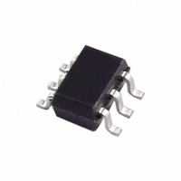
ADG741BKS-REEL7 Analog Devices Inc, ADG741BKS-REEL7 Datasheet - Page 3

ADG741BKS-REEL7
Manufacturer Part Number
ADG741BKS-REEL7
Description
IC SWITCH SPST SC70-6
Manufacturer
Analog Devices Inc
Datasheet
1.ADG742BKSZ-REEL.pdf
(12 pages)
Specifications of ADG741BKS-REEL7
Rohs Status
RoHS non-compliant
Function
Switch
Circuit
1 x SPST- NC
On-state Resistance
3 Ohm
Voltage Supply Source
Single Supply
Voltage - Supply, Single/dual (±)
1.8 V ~ 5.5 V
Operating Temperature
-40°C ~ 85°C
Mounting Type
Surface Mount
Package / Case
6-TSSOP, SC-88, SOT-363
Available stocks
Company
Part Number
Manufacturer
Quantity
Price
Company:
Part Number:
ADG741BKS-REEL7
Manufacturer:
MAXIM
Quantity:
27
Part Number:
ADG741BKS-REEL7
Manufacturer:
ADI/亚德诺
Quantity:
20 000
SPECIFICATIONS
V
Table 1.
Parameter
ANALOG SWITCH
LEAKAGE CURRENTS
DIGITAL INPUTS
DYNAMIC CHARACTERISTICS
POWER REQUIREMENTS
1
Guaranteed by design; not subject to production test.
DD
Analog Signal Range
On Resistance (R
On Resistance Flatness (R
Source OFF Leakage I
Drain OFF Leakage I
Channel ON Leakage I
Input High Voltage, V
Input Low Voltage, V
Input Current
t
t
Charge Injection
Off Isolation
Bandwidth −3 dB
C
C
C
I
DD
ON
OFF
S
D
D
= 5 V ±10%, GND = 0 V. All specifications −40°C to +85°C, unless otherwise noted.
I
, C
(OFF)
(OFF)
INL
S
or I
(ON)
INH
ON
1
)
D
INL
INH
S
(OFF)
D
(OFF)
, I
S
FLAT (ON)
(ON)
1
)
25°C
2
3
0.5
±0.01
±0.25
±0.01
±0.25
±0.01
±0.25
0.005
12
8
5
−55
−75
200
17
17
38
0.001
B Version
−40°C to +85°C
0 V to V
4
1.0
±0.35
±0.35
±0.35
2.4
0.8
±0.1
18
12
1.0
Rev. A | Page 3 of 12
DD
Unit
V
Ω typ
Ω max
Ω typ
Ω max
nA typ
nA max
nA typ
nA max
nA typ
nA max
V min
V max
µA typ
µA max
ns typ
ns max
ns typ
ns max
pC typ
dB typ
dB typ
MHz typ
pF typ
pF typ
pF typ
µA typ
µA max
Test Conditions/Comments
V
Figure 11
V
V
V
Figure 12
V
Figure 12
V
Figure 13
V
R
V
R
V
V
RL = 50 Ω, C
R
R
V
Digital Inputs = 0 V or 5 V
S
S
DD
S
S
S
IN
L
S
L
S
S
L
L
DD
= 0 V to V
= 0 V to V
= 4.5 V/1 V, V
= 4.5 V/1 V, V
= V
= 300 Ω, C
= 3 V; Figure 14
= 300 Ω, C
= 3 V; Figure 14
= 2 V, R
= 50 Ω, C
= 50 Ω, C
= V
= 5.5 V
= 5.5 V
D
INL
= 1 V, or 4.5 V;
or V
S
= 0 Ω, C
L
L
DD
DD
L
= 5 pF, f = 1 MHz; Figure 16
= 5 pF; Figure 17
L
L
INH
= 5 pF, f = 10 MHz
= 35 pF
= 35 pF
, I
, I
D
D
S
S
= −10 mA;
= −10 mA
= 1 V/4.5 V;
= 1 V/4.5 V;
L
= 1 nF; Figure 15
ADG741/ADG742


