ADG759BCP Analog Devices Inc, ADG759BCP Datasheet

IC MULTIPLEXER DUAL 4X1 20LFCSP

ADG759BCP

Manufacturer Part Number
ADG759BCP
Description
IC MULTIPLEXER DUAL 4X1 20LFCSP
Manufacturer
Analog Devices Inc
Datasheet

Specifications of ADG759BCP

Rohs Status
RoHS non-compliant
Function
Multiplexer
Circuit
2 x 4:1
On-state Resistance
4.5 Ohm
Voltage Supply Source
Single, Dual Supply
Voltage - Supply, Single/dual (±)
1.8 V ~ 5.5 V, ±2.5 V
Current - Supply
0.001µA
Operating Temperature
-40°C ~ 85°C
Mounting Type
Surface Mount
Package / Case
20-VFQFN, CSP Exposed Pad

Available stocks

Company
Part Number
Manufacturer
Quantity
Price
Part Number:
ADG759BCP
Manufacturer:
ADI/亚德诺
Quantity:
20 000
a
REV. A
Information furnished by Analog Devices is believed to be accurate and
reliable. However, no responsibility is assumed by Analog Devices for its
use, nor for any infringements of patents or other rights of third parties that
may result from its use. No license is granted by implication or otherwise
under any patent or patent rights of Analog Devices.
GENERAL DESCRIPTION
The ADG758 and ADG759 are low voltage, CMOS analog
multiplexers comprising eight single channels and four differential
channels, respectively. The ADG758 switches one of eight inputs
(S1–S8) to a common output, D, as determined by the 3-bit
binary address lines A0, A1, and A2. The ADG759 switches one
of four differential inputs to a common differential output as
determined by the 2-bit binary address lines A0 and A1. An EN
input on both devices is used to enable or disable the device. When
disabled, all channels are switched OFF.
Low power consumption and an operating supply range of 1.8 V to
5.5 V make the ADG758 and ADG759 ideal for battery-powered,
portable instruments. All channels exhibit break-before-make
switching action preventing momentary shorting when switch-
ing channels.
These switches are designed on an enhanced submicron process
that provides low power dissipation yet gives high switching
speed, very low ON resistance and leakage currents. ON resistance
is in the region of a few ohms and is closely matched between
switches and very flat over the full signal range. These parts can
operate equally well as either multiplexers or demultiplexers
and have an input signal range that extends to the supplies.
The ADG758 and ADG759 are available in 20-lead chip
scale packages.
FEATURES
1.8 V to 5.5 V Single Supply
3
0.75
100 pA Leakage Currents
14 ns Switching Times
Single 8-to-1 Multiplexer ADG758
Differential 4-to-1 Multiplexer ADG759
20-Lead 4 mm
Low Power Consumption
TTL-/CMOS-Compatible Inputs
For Functionally Equivalent Devices in 16-Lead TSSOP
APPLICATIONS
Data Acquisition Systems
Communication Systems
Relay Replacement
Audio and Video Switching
Battery-Powered Systems
2.5 V Dual Supply
Package, See ADG708/ADG709
ON Resistance
ON Resistance Flatness
4 mm Chip Scale Package
PRODUCT HIGHLIGHTS
1. Small 20-Lead 4 mm × 4 mm Chip Scale Packages (CSP).
2. Single/Dual Supply Operation. The ADG758 and ADG759
3. Low R
4. Low Power Consumption (<0.01 µW).
5. Guaranteed Break-Before-Make Switching Action.
One Technology Way, P.O. Box 9106, Norwood, MA 02062-9106, U.S.A.
Tel: 781/329-4700
Fax: 781/326-8703
3 , 4-/8-Channel Multiplexers
are fully specified and guaranteed with 3 V and 5 V single-
supply and ± 2.5 V dual-supply rails.
S1
S8
ON
A0
FUNCTIONAL BLOCK DIAGRAMS
(3 Ω Typical).
ADG758
DECODER
A1
1 OF 8
in Chip Scale Package
A2
EN
ADG758/ADG759
D
S4A
S1B
S4B
S1A
© Analog Devices, Inc., 2002
A0
ADG759
DECODER
1 OF 4
A1
EN
www.analog.com
DA
DB

Related parts for ADG759BCP

ADG759BCP Summary of contents

Page 1

FEATURES 1 5.5 V Single Supply 2.5 V Dual Supply 3 ON Resistance 0.75 ON Resistance Flatness 100 pA Leakage Currents 14 ns Switching Times Single 8-to-1 Multiplexer ADG758 Differential 4-to-1 Multiplexer ADG759 20-Lead ...

Page 2

ADG758/ADG759–SPECIFICATIONS Parameter ANALOG SWITCH Analog Signal Range ON Resistance ( Resistance Match Between Channels (∆ Resistance Flatness (R ) FLAT(ON) LEAKAGE CURRENTS Source OFF Leakage I (OFF) S Drain OFF Leakage I (OFF) D ...

Page 3

SPECIFICATIONS (V DD Parameter ANALOG SWITCH Analog Signal Range ON Resistance ( Resistance Match Between Channels (∆ LEAKAGE CURRENTS Source OFF Leakage I (OFF) S Drain OFF Leakage I (OFF) D Channel ON Leakage ...

Page 4

ADG758/ADG759–SPECIFICATIONS DUAL SUPPLY (V = +2 Parameter ANALOG SWITCH Analog Signal Range ON Resistance ( Resistance Match Between Channels (∆ Resistance Flatness (R ) FLAT(ON) LEAKAGE CURRENTS Source OFF Leakage ...

Page 5

... X = Don’t Care Model Temperature Range ADG758BCP –40°C to +85°C ADG759BCP –40°C to +85°C REV. A Chip Scale Package, θ Thermal Impedance . . . . . . . . . . . . . . . . . . . . . . 32°C/W JA Lead Temperature, Soldering Vapor Phase (60 sec 215°C Infrared (15 sec 220°C – NOTES DD 1 Stresses above those listed under Absolute Maximum Ratings may cause perma- nent damage to the device. This is a stress rating only ...

Page 6

ADG758/ADG759 V Most Positive Power Supply Potential DD V Most Negative Power Supply in a dual-supply application. In single-supply applications, this should be tied to SS ground at the device. GND Ground (0 V) Reference S Source Terminal. May be ...

Page 7

DRAIN OR SOURCE VOLTAGE – TPC 1. ON Resistance as a ...

Page 8

ADG758/ADG759 0.12 0.08 0.04 0.00 I (OFF) –0.04 S –0.08 –0.12 0 0.5 1.0 1 – TPC 7. Leakage Currents as a Function of V 0.12 0.08 I 0.04 D ...

Page 9

FREQUENCY – Hz TPC 13. Crosstalk vs. Frequency –5 –10 –15 –20 30k 100k 1M FREQUENCY – Hz TPC 14. ...

Page 10

ADG758/ADG759 Test Circuits Test Circuit 1. ON Resistance (OFF GND D ...

Page 11

THRU S8 ADG758* EN GND *SIMILAR CONNECTION FOR ADG759 ADG758 GND IN *SIMILAR ...

Page 12

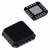
ADG758/ADG759 PIN 1 INDICATOR 0.035 (0.90) MAX 0.033 (0.85) NOM SEATING PLANE Revision History Location Data Sheet changed from REV REV. A. Edits to General Description section . . . . . . . . . . . ...

Related keywords