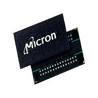
MT46V32M16BN-6:FTR Micron Technology Inc, MT46V32M16BN-6:FTR Datasheet - Page 86

MT46V32M16BN-6:FTR
Manufacturer Part Number
MT46V32M16BN-6:FTR
Description
Manufacturer
Micron Technology Inc
Datasheet
1.MT46V32M16BN-6FTR.pdf
(91 pages)
Specifications of MT46V32M16BN-6:FTR
Lead Free Status / Rohs Status
Compliant
- Current page: 86 of 91
- Download datasheet (4Mb)
Figure 51:
PDF: 09005aef80a1d9d4/Source: 09005aef82a95a3a
DDR_x4x8x16_Core2.fm - 512Mb DDR: Rev. N; Core DDR Rev. B 2/09 EN
Case 1: t AC (MIN) and t DQSCK (MIN)
Case 2: t AC (MAX) and t DQSCK (MAX)
Command
BA0, BA1
Address
DQ
DQ
DQS
DQS
CK#
CKE
A10
DM
CK
6
6
Bank READ – with Auto Precharge
t IS
t IS
NOP
T0
t IH
1
t IH
Notes:
Bank x
IS
t IS
Row
ACT
Row
1. NOP commands are shown for ease of illustration; other commands may be valid at these
2. BL = 4.
3. The READ command can only be applied at T3 if
4. Enable auto precharge.
5.
6. DO n = data-out from column n; subsequent elements are provided in the programmed
7. Refer to Figure 35 on page 70, Figure 36 on page 71, and Figure 37 on page 72 for detailed
T1
IH
t IH
times.
t
order.
DQS and DQ timing.
t CK
RP starts only after
t RCD, t RAP 3
t RAS
t RC
NOP
T2
1
t CH
t CL
t IS
READ
Bank x
4
Col n
t
RAS has been satisfied.
T3
t IH
2,3
t LZ (MIN)
CL = 2
86
NOP
T4
t RPRE
1
t LZ (MIN)
Micron Technology, Inc., reserves the right to change products or specifications without notice.
t RPRE
NOP
T5
t DQSCK (MIN)
DO
t DQSCK (MAX)
1
n
512Mb: x4, x8, x16 DDR SDRAM
t AC (MIN)
DO
t
n
t AC (MAX)
RAP is satisfied at T3.
T5n
t RP 5
NOP
T6
Transitioning Data
1
t HZ (MAX)
T6n
t RPST
©2000 Micron Technology, Inc. All rights reserved.
t RPST
NOP
T7
1
Operations
Don’t Care
Bank x
ACT
T8
Row
Row
Related parts for MT46V32M16BN-6:FTR
Image
Part Number
Description
Manufacturer
Datasheet
Request
R

Part Number:
Description:
IC SDRAM 64MBIT 133MHZ 54TSOP
Manufacturer:
Micron Technology Inc
Datasheet:

Part Number:
Description:
IC SDRAM 64MBIT 5.5NS 86TSOP
Manufacturer:
Micron Technology Inc
Datasheet:

Part Number:
Description:
IC SDRAM 64MBIT 200MHZ 86TSOP
Manufacturer:
Micron Technology Inc
Datasheet:

Part Number:
Description:
IC SDRAM 64MBIT 133MHZ 54TSOP
Manufacturer:
Micron Technology Inc
Datasheet:

Part Number:
Description:
IC SDRAM 128MBIT 133MHZ 54TSOP
Manufacturer:
Micron Technology Inc
Datasheet:

Part Number:
Description:
IC SDRAM 256MBIT 133MHZ 90VFBGA
Manufacturer:
Micron Technology Inc
Datasheet:

Part Number:
Description:
IC SDRAM 128MBIT 133MHZ 54TSOP
Manufacturer:
Micron Technology Inc
Datasheet:

Part Number:
Description:
IC SDRAM 256MBIT 133MHZ 54TSOP
Manufacturer:
Micron Technology Inc
Datasheet:

Part Number:
Description:
IC DDR SDRAM 512MBIT 6NS 66TSOP
Manufacturer:
Micron Technology Inc
Datasheet:

Part Number:
Description:
IC SDRAM 128MBIT 167MHZ 86TSOP
Manufacturer:
Micron Technology Inc
Datasheet:

Part Number:
Description:
IC SDRAM 128MBIT 143MHZ 86TSOP
Manufacturer:
Micron Technology Inc
Datasheet:

Part Number:
Description:
SDRAM 256M-BIT 1.8V 54-PIN VFBGA
Manufacturer:
Micron Technology Inc
Datasheet:

Part Number:
Description:
IC SDRAM 128MBIT 143MHZ 86TSOP
Manufacturer:
Micron Technology Inc
Datasheet:

Part Number:
Description:
IC SDRAM 128MBIT 125MHZ 54VFBGA
Manufacturer:
Micron Technology Inc
Datasheet:

Part Number:
Description:
IC SDRAM 128MBIT 125MHZ 54VFBGA
Manufacturer:
Micron Technology Inc
Datasheet:


