STV6412AD STMicroelectronics, STV6412AD Datasheet - Page 11
STV6412AD
Manufacturer Part Number
STV6412AD
Description
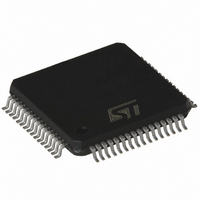
IC AUDIO/VIDEO SWIT DUAL 64TQFP
Manufacturer
STMicroelectronics
Datasheet
1.STV6412AD.pdf
(31 pages)
Specifications of STV6412AD
Function
Audio/Video Switch
Circuit
2 x SCART
Voltage Supply Source
Single Supply
Voltage - Supply, Single/dual (±)
4.75 V ~ 5.25 V, 11.2 V ~ 12.8 V
Current - Supply
43mA
Operating Temperature
0°C ~ 70°C
Mounting Type
Surface Mount
Package / Case
64-TQFP, 64-VQFP
Lead Free Status / RoHS Status
Lead free / RoHS Compliant
Available stocks
Company
Part Number
Manufacturer
Quantity
Price
Company:

Part Number:
STV6412AD
Manufacturer:
STMicroelectronics
Quantity:
10 000
Part Number:
STV6412AD
Manufacturer:
ST
Quantity:
20 000
Company:
Part Number:
STV6412ADT
Manufacturer:
LRC
Quantity:
2 117
Company:
Part Number:
STV6412ADT
Manufacturer:
STMicroelectronics
Quantity:
10 000
Part Number:
STV6412ADT
Manufacturer:
ST
Quantity:
20 000


STV6412A
Table 6.
Note:
DC
G
G
Flatness Spread of gain in video band
Symbol
G
G
DC
I
V
YCVBSM
CLAMP
G
RGBSTE
I
R
DPHI
DYN
YCVBS
LEAK
CTo
Mute
BW
CTi
RGBM
VSN
C
V
OUT RF
LNL
DCIN
DG
OUT
RGB
P
OUT
IN
IN
1
DC input level
Clamping current
Input leakage current
Input capacitance
Max input signal
Dynamic output signal
Bandwidth at -3 dB
(15 kHz - 5 MHz)
Crosstalk isolation between input
channel
Crosstalk isolation between output
channel
Output resistance
Gain at RGB outputs
Gain matching between R, G, B
Step of gain
Gain on Y,/CVBS channels
Gain matching between Y, CVBS
inputs
DC output voltage
RF output voltage
Differential phase
Differential gain
Mute suppression
Luminance non-linerarity
Video S/N ratio
Video section characteristics
S/N = 20 log (V
Y/C mixer (on VOUT-RF)
Y/C Mixer (on VOUT-RF)
Y/CVBS
RGB
Y/CVBS
RGB
Parameter
OUT
Black to White = 0.7 V
Doc ID 9754 Rev 2
Bottom synch pulse
at VDCIN -400 mV
VIN = VDCIN +1 V
VCC = 5 V
VCC = 5 V
VIN = 1 VPP
VIN = 1 VPP
VIN = 1 VPP, VINC = muted
VIN = 1 VPP
VIN = 1 VPP
VIN = 1 VPP, VINC = muted
VIN = 1 VPP at f = 4.43 MHz,
on one point
VIN = 1 VPP at f = 4.43 MHz,
on one point, RLOAD = 150Ω
V
V
3 dB to 6 dB
V
V
Bottom sync pulse
Bottom sync pulse
V
V
V
point
Refer to
IN
IN
IN
IN
IN
IN
IN
= 1 V
= 1 V
= 1 V
= 1 V
= 1 V
= 1 V
= 1 V
Note 1
pp,
PP,
PP
PP
PP
PP
PP
Test condition
PP
gain set to 6 dB
at f = 4.43 MHz
at f = 4.43 MHz
at f = 5 MHz on one
gain set to 6 dB
/ V
Noise
(mV
RMS
) weighted CCIR 567).
Electrical characteristics
Min.
0.75
-55
-0.3
-0.5
12
12
5.5
5.5
65
1
8
Typ.
1.5
0.3
0.6
15
15
10
60
50
2
2
1
2
3
5
1
1
1
6
0
1
6
0
+/-0.5
+/-0.5
+/-1.5
Max.
1.25
10
10
6.5
0.3
6.5
0.5
5
5
3
° deg.
MHz
MHz
MHz
Unit
V
V
11/31
mA
µA
pF
dB
dB
dB
dB
dB
dB
dB
dB
dB
dB
dB
dB
%
Ω
%
V
V
V
PP
PP
Related parts for STV6412AD
Image
Part Number
Description
Manufacturer
Datasheet
Request
R

Part Number:
Description:
STMicroelectronics [RIPPLE-CARRY BINARY COUNTER/DIVIDERS]
Manufacturer:
STMicroelectronics
Datasheet:
Part Number:
Description:
STMicroelectronics [LIQUID-CRYSTAL DISPLAY DRIVERS]
Manufacturer:
STMicroelectronics
Datasheet:

Part Number:
Description:
BOARD EVAL FOR MEMS SENSORS
Manufacturer:
STMicroelectronics
Datasheet:
Part Number:
Description:
NPN TRANSISTOR POWER MODULE
Manufacturer:
STMicroelectronics
Datasheet:
Part Number:
Description:
TURBOSWITCH ULTRA-FAST HIGH VOLTAGE DIODE
Manufacturer:
STMicroelectronics
Datasheet:
Part Number:
Description:
Manufacturer:
STMicroelectronics
Datasheet:
Part Number:
Description:
DIODE / SCR MODULE
Manufacturer:
STMicroelectronics
Datasheet:
Part Number:
Description:
DIODE / SCR MODULE
Manufacturer:
STMicroelectronics
Datasheet:
Part Number:
Description:
Search -----> STE16N100
Manufacturer:
STMicroelectronics
Datasheet:
Part Number:
Description:
Search ---> STE53NA50
Manufacturer:
STMicroelectronics
Datasheet:
Part Number:
Description:
NPN Transistor Power Module
Manufacturer:
STMicroelectronics
Datasheet:
Part Number:
Description:
DIODE / SCR MODULE
Manufacturer:
STMicroelectronics
Datasheet: