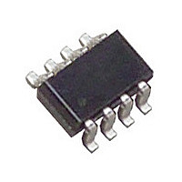
LTC2912CTS8-3#PBF Linear Technology, LTC2912CTS8-3#PBF Datasheet - Page 3

LTC2912CTS8-3#PBF
Manufacturer Part Number
LTC2912CTS8-3#PBF
Description
Manufacturer
Linear Technology
Datasheet
1.LTC2912CTS8-3PBF.pdf
(12 pages)
Specifications of LTC2912CTS8-3#PBF
Voltage Supervisor Type
Voltage Monitor
Number Of Voltage Supervisors
1
Monitored Supervisor Voltage
3.3
Reset Threshold Voltage (min)
AdjV
Reset Threshold Voltage (max)
AdjV
Operating Supply Voltage (min)
2.3V
Operating Supply Voltage (max)
6V
Package Type
TSOT-23
Operating Temperature Classification
Commercial
Operating Temp Range
0C to 70C
Pin Count
8
Mounting
Surface Mount
Lead Free Status / Rohs Status
Compliant
Available stocks
Company
Part Number
Manufacturer
Quantity
Price
ELECTRICAL CHARACTERISTICS
SYMBOL
V
ΔV
V
V
V
ΔV
I
V
t
I
t
V
V
I
I
V
V
I
I
V
V
V
Note 1: Stresses beyond those listed under Absolute Maximum Ratings
may cause permanent damage to the device. Exposure to any Absolute
Maximum Rating condition for extended periods may affect device
reliability and lifetime.
Note 2: All currents into pins are positive; all voltages are referenced to
GND unless otherwise noted.
temperature range, otherwise specifi cations are at T
noted. (Note 2)
CC
UOD
VHL
UOTO
LATCH
DIS
TMR(UP)
TMR(DOWN)
TMR(DIS)
SHUNT
CC
CCR(MIN)
CC(UVLO)
UOT
LATCH(VIH)
LATCH(VIL)
DIS(VIH)
DIS(VIL)
OH
OL
SHUNT
CC(UVHYST)
PARAMETER
V
V
Supply Voltage (Note 3)
Minimum V
Supply Undervoltage Lockout
Supply Undervoltage Lockout Hysteresis
Supply Current
Undervoltage/Overvoltage Threshold
Undervoltage/Overvoltage Threshold to
Output Delay
VH, VL Input Current
UV/OV Time-Out Period
OV Latch Clear Input High
OV Latch Clear Input Low
LATCH Input Current
DIS Input Current
DIS Input High
DIS Input Low
TMR Pull-Up Current
TMR Pull-Down Current
Timer Disable Voltage
Output Voltage High UV/OV/OV
Output Voltage Low UV/OV/OV
CC
CC
Shunt Regulator Voltage
Shunt Regulator Load Regulation
CC
Output Valid
A
= 25°C. V
CONDITIONS
I
–40°C < T
I
DIS = 0V
DIS = 0V, V
DIS = 0V
V
V
–40°C < T
C
–40°C < T
V
V
V
–40°C < T
V
–40°C < T
Referenced to V
V
V
V
CC
CC
TMR
TMR
CC
Hn
TMR
LATCH
DIS
CC
CC
CC
= 5mA
= 2mA to 10mA
= 2.3V to 6V
= V
= 2.3V, I
= 2.3V, I
= 1V, I
The
> 0.5V
= 0V
= 1.6V
= 1nF
> 0.5V
UOT
●
A
A
A
A
A
CC
UV
CC
< 125°
– 5mV or V
< 125°
< 125°
< 125°
< 125°
denotes the specifi cations which apply over the full operating
UV/OV
UV/OV
= 3.3V, VL = 0.45V, VH = 0.55V, LATCH = V
= 100μA
Rising
CC
Note 3: V
V
exceeds 6V may exceed the rated terminal current. Operation from higher
voltage supplies requires a series dropping resistor. See Applications
Information.
= –1μA
= 2.5mA
CC
pin has an internal 6.5V shunt regulator, a low impedance supply that
Ln
= V
CC
UOT
maximum pin voltage is limited by input current. Since the
+ 5mV
●
●
●
●
●
●
●
●
●
●
●
●
●
●
●
●
●
●
●
●
●
●
●
●
●
●
●
●
–180
–1.3
–1.2
MIN
492
6.2
6.2
2.3
1.9
1.2
1.2
1.3
1.2
50
5
6
6
1
1
CC
–270
–2.1
–2.1
0.10
0.01
TYP
200
500
125
unless otherwise
6.6
6.6
8.5
8.5
2.1
2.1
25
29
2
2
LTC2912
V
MAX
SHUNT
12.5
–2.8
–2.8
0.30
0.15
300
508
500
±15
±30
7.2
7.3
2.1
0.8
3.3
0.8
2.8
2.8
50
70
14
±1
1
UNITS
3
2912fa
mV
mV
mV
mV
ms
ms
μA
nA
nA
μA
μA
μA
μA
μA
μA
μs
V
V
V
V
V
V
V
V
V
V
V
V


