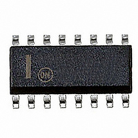
MC74HC4051ADWG ON Semiconductor, MC74HC4051ADWG Datasheet - Page 5

MC74HC4051ADWG
Manufacturer Part Number
MC74HC4051ADWG
Description
IC MUX/DEMUX 8X1 16SOIC
Manufacturer
ON Semiconductor
Series
74HCr
Type
Analog Multiplexerr
Datasheet
1.MC74HC4053ANG.pdf
(18 pages)
Specifications of MC74HC4051ADWG
Function
Multiplexer/Demultiplexer
Circuit
1 x 8:1
On-state Resistance
100 Ohm
Voltage Supply Source
Single, Dual Supply
Voltage - Supply, Single/dual (±)
±2 V ~ 6 V, 2 V ~ 12 V
Current - Supply
40µA
Operating Temperature
-55°C ~ 125°C
Mounting Type
Surface Mount
Package / Case
16-SOIC (0.300", 7.50mm Width)
On Resistance (max)
190 Ohms
Propagation Delay Time
40 ns
On Time (max)
245 ns
Off Time (max)
160 ns
Supply Voltage (max)
6 V
Supply Voltage (min)
2 V
Maximum Power Dissipation
500 mW
Maximum Operating Temperature
+ 125 C
Minimum Operating Temperature
- 55 C
Mounting Style
SMD/SMT
Number Of Switches
Single
Number Of Channels
1 Channel
Number Of Lines (input / Output)
8 / 1
Lead Free Status / RoHS Status
Lead free / RoHS Compliant
Other names
MC74HC4051ADWG
MC74HC4051ADWGOS
MC74HC4051ADWGOS
NOTE: For propagation delays with loads other than 50 pF, and information on typical parametric values, see Chapter 2 of the ON
* Used to determine the no-load dynamic power consumption: P
DC CHARACTERISTICS — Analog Section
AC CHARACTERISTICS
Symbol
Symbol
ON Semiconductor High-Speed CMOS Data Book (DL129/D).
DR
t
t
t
t
t
t
t
t
C
C
R
PLH
PLH
PLZ
PZL
PHL
PHL
PHZ
PZH
C
I
I
off
on
I/O
PD
on
in
on
,
,
,
,
Semiconductor High-Speed CMOS Data Book (DL129/D)
Maximum “ON” Resistance
Maximum Difference in “ON”
Resistance Between Any Two
Channels in the Same Package
Maximum Off-Channel Leakage
Current, Any One Channel
Maximum Off-ChannelHC4051A
Leakage Current,
Common Channel
Maximum On-ChannelHC4051A
Leakage Current,
Channel-to-Channel HC4053A
Maximum Propagation Delay, Channel-Select to Analog Output
(Figure 9)
Maximum Propagation Delay, Analog Input to Analog Output
(Figure 10)
Maximum Propagation Delay, Enable to Analog Output
(Figure 11)
Maximum Propagation Delay, Enable to Analog Output
(Figure 11)
Maximum Input Capacitance, Channel-Select or Enable Inputs
Maximum Capacitance
(All Switches Off)
Power Dissipation Capacitance (Figure 13)*
Parameter
(C
L
MC74HC4051A, MC74HC4052A, MC74HC4053A
= 50 pF, Input t
HC4052A
HC4053A
HC4052A
Parameter
V
V
(Figures 1, 2)
V
V
(Figures 1, 2)
V
V
I
V
V
Switch Off (Figure 3)
V
V
Switch Off (Figure 4)
V
Switch-to-Switch =
V
S
in
EE
in
EE
in
IS
in
IO
in
IO
in
CC
r
≤ 2.0 mA
= t
= V
= V
= V
= V
= V
= V
; I
= 1/2 (V
= V
= V
(Endpoints); I
- V
f
S
= 6 ns)
IL
IL
IL
IL
IL
IL
CC
CC
≤ 2.0 mA
EE
Common O/I: HC4051A
or V
or V
or V
or V
or V
or V
Condition
; (Figure 5)
- V
- V
http://onsemi.com
CC
IH
IH
IH
IH
IH
IH
EE
EE
; V
; V
;
- V
;
;
;
;
;
IS
IS
S
Feed-through
EE
D
≤ 2.0 mA
= V
= V
);
= C
Analog I/O
5
HC4052A
HC4053A
CC
CC
PD
to
or
V
HC4051A
HC4052A
HC4053A
CC
2
f + I
V
4.5
4.5
6.0
4.5
4.5
6.0
4.5
4.5
6.0
6.0
6.0
6.0
6.0
6.0
6.0
6.0
CC
CC
V
CC
Typical @ 25°C, V
- 4.5
- 6.0
- 4.5
- 6.0
- 4.5
- 6.0
- 6.0
- 6.0
- 6.0
- 6.0
- 6.0
- 6.0
- 6.0
V
V
0.0
0.0
0.0
2.0
3.0
4.5
6.0
2.0
3.0
4.5
6.0
2.0
3.0
4.5
6.0
2.0
3.0
4.5
6.0
V
CC
EE
. For load considerations, see Chapter 2 of the
-55 to 25°C
-55 to 25°C
190
120
100
150
100
270
160
245
115
130
0.1
0.2
0.1
0.1
0.2
0.1
0.1
1.0
80
30
12
10
90
59
45
40
25
12
10
70
48
39
49
39
10
35
80
50
Guaranteed Limit
Guaranteed Limit
CC
45
80
45
= 5.0 V, V
≤85°C
≤85°C
240
150
125
190
125
100
320
110
200
315
145
130
0.5
2.0
1.0
1.0
2.0
1.0
1.0
1.0
35
15
12
79
65
60
30
15
13
95
63
55
69
58
10
35
80
50
EE
≤125°C
≤125°C
= 0 V
280
170
140
230
140
350
125
220
345
155
130
115
110
1.0
4.0
2.0
2.0
4.0
2.0
2.0
1.0
40
18
14
85
75
70
32
18
15
76
63
83
67
10
35
80
50
Unit
Unit
mA
mA
pF
pF
pF
ns
ns
ns
ns
W
W


