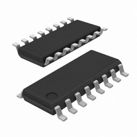
SI3200-BS Silicon Laboratories Inc, SI3200-BS Datasheet - Page 7

SI3200-BS
Manufacturer Part Number
SI3200-BS
Description
IC LINEFEED INTRFC 100V 16SOIC
Manufacturer
Silicon Laboratories Inc
Series
ProSLIC®r
Specifications of SI3200-BS
Function
Subscriber Line Interface Concept (SLIC), CODEC
Interface
GCI, PCM, SPI
Number Of Circuits
2
Voltage - Supply
3.3V, 5V
Current - Supply
110µA
Power (watts)
941mW
Operating Temperature
-40°C ~ 85°C
Mounting Type
Surface Mount
Package / Case
16-SOIC (3.9mm Width)
Includes
Battery Switching, BORSCHT Functions, DTMF Generation and Decoding, FSK Tone Generation, Modem and Fax Tone Detection
Lead Free Status / RoHS Status
Contains lead / RoHS non-compliant
Available stocks
Company
Part Number
Manufacturer
Quantity
Price
Company:
Part Number:
SI3200-BS
Manufacturer:
SILICON
Quantity:
1 082
Part Number:
SI3200-BS
Manufacturer:
N/A
Quantity:
20 000
Company:
Part Number:
SI3200-BSR
Manufacturer:
SILICON
Quantity:
14 000
(choose 0.75 W or 1 W resistor – typically in a 2010
package size for SMT or use a through-hole resistor)
For Linear Regulator offload:
Vz = |–56 V| – |–36 V| – 0.6 V = 19.4 V
(choose 19 V or 20 V 5% Zener diode).
Figure 1 depicts the ON Semiconductor MJD2955
(DPAK)
CMPZ4707 (SOT-23) 20 V Zener diode, which are well
suited for the constraints of this example. The MJD2955
transistor, when installed on the manufacturer’s
recommended minimum PCB pad size, provides
P
ambient temperatures above 25 °C. Thus, at Ta = 85°C,
the transistor with its minimum specified PCB pad is
rated
The following equation gives the expected off-hook
transistor power dissipation:
P
0.985W
The
(V
Forward Bias Safe Operating Area” given by the
transistor manufacturer, which typically assumes that
the transistor is mounted on an “infinite” heat sink
(T
However, P
0.91 W at 85 °C, which is based on the minimum pad
size shown in the manufacturer’s data sheet. Therefore,
the pad size for the transistor must be increased from
the minimum size recommended by the transistor
manufacturer in order to ensure that the transistor’s
junction temperature will remain below 150 °C when
operating at Ta = 85 °C and while dissipating the
nominal 985 mW plus a reasonable safety margin.
For the MJD2955 transistor, heat is primarily dissipated
via the paddle of the DPAK package, which is
electrically connected to the collector. The minimum pad
size recommended by the manufacturer for the paddle
is 4.826 mm x 4.191 mm, which yields θ
This minimum collector pad size must be enhanced
sufficiently to provide enough heat dissipation in order
to reduce the resulting θ
θ
/ 0.985 W = 66 °C; use 60 °C/W for added margin).
Generally, the effective θ
the size of PCB heat slug pad for the transistor paddle
and/or by tying the PCB component-side heat slug
copper pad to copper fill on other PCB layers using
multiple vias.
The final PCB heat slug design must be verified by
25 °C) = 0.91 W.
ja(max)
d(max)
Q
c
CE
= 2 x (56V – 36V) x (0.020625A + 0.004A) =
= 25 °C).
= 20 V, I
nominal
= 1.75 W at 25 °C and derates by 0.014 W/°C at
= (T
at
transistor
Q
j(max)
1.75 W
C
exceeds the transistor’s derated P
= 49.25 mA) is well within the “Maximum
operating
– T
a(max)
and
–
ja
) / P
will be reduced by increasing
0.014 W/°C
point
ja
Central
d(max)
below 60 °C/W (i.e.
for
= (150 °C – 85 °C)
Semiconductor
the
ja
= 71.4 °C/W.
x
transistor
(85 °C –
d(max)
Rev. 0.1
of
measuring the actual θ
less.
The following equation gives the worst-case Zener
diode power dissipation:
P
The diode manufacturer’s data sheet states a rating of
T
estimated thermal resistance of a Zener diode in an
SOT-23 package is 500 °C/W.
The junction temperature of the diode can be estimated
as: T
Tj = 500 °C/W x 0.050 W + 85 °C = 110 °C
which is well below T
5. Calculate the correct values for BATHTH, BATLTH, and
V
BATHTH = 2
1) = 0x1A00
BATLTH = 2
1) = 0x1900
BATHLPF = 2
800) = 0xA10
Figure 3. Si3200 Power Calculation (example)
j(max)
Z
thres
= 2 x 20 V x (0.020625 A + 0.004 A) / 20 = 0.050 W
BATLPF using Equations 13, 14, 15, and 16:
1.1
0.9
0.8
0.7
0.6
0.5
0.4
0.3
0.2
0.1
j
1
0
= θ
= 36 V – 4 V = 32 V
= 150 °C and P
ja
x P
7
7
3
d
x DEC2HEX ((2 x 3.14159 x 10 x 4096) /
+ T
x
x
a
, which yields:
DEC2HEX
DEC2HEX
Loop Length (feet)
j
(max) = 150 °C.
d(max)
ja
and verifying it is 60 °C/W or
= 350 mW @ 25 °C. The
(
(
(32V/0.628 V)
(32V/0.628 V)
P slic
M ax P slic
AN91
+
–
7


