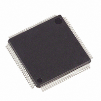
DS21352L Maxim Integrated Products, DS21352L Datasheet - Page 69

DS21352L
Manufacturer Part Number
DS21352L
Description
IC TXRX T1 1-CHIP 3.3V 100-LQFP
Manufacturer
Maxim Integrated Products
Datasheet
1.DS21352L.pdf
(137 pages)
Specifications of DS21352L
Function
Single-Chip Transceiver
Interface
HDLC, T1
Number Of Circuits
1
Voltage - Supply
3.14 V ~ 3.47 V
Current - Supply
75mA
Operating Temperature
0°C ~ 70°C
Mounting Type
Surface Mount
Package / Case
100-LQFP
Includes
DSX-1 and CSU Line Build-Out Generator, HDLC Controller, In-Band Loop Code Generator and Detector
Lead Free Status / RoHS Status
Contains lead / RoHS non-compliant
Power (watts)
-
Available stocks
Company
Part Number
Manufacturer
Quantity
Price
Company:
Part Number:
DS21352L
Manufacturer:
JRC
Quantity:
5 510
Part Number:
DS21352L
Manufacturer:
DALLAS
Quantity:
20 000
Company:
Part Number:
DS21352LN+
Manufacturer:
Maxim Integrated Products
Quantity:
135
Like the SR1 and SR2 status registers, the HSR register has the unique ability to initiate a hardware
interrupt via the INT* output pin. Each of the events in the HSR can be either masked or unmasked from
the interrupt pin via the HDLC Interrupt Mask Register (HIMR). Interrupts will force the INT* pin low
when the event occurs. The INT pin will be allowed to return high (if no other interrupts are present)
when the user reads the event bit that caused the interrupt to occur.
15.3.3 BASIC OPERATION DETAILS
To allow the framer to properly source/receive data from/to the HDLC and BOC controller the legacy FDL circuitry (which is
described in Section 15.4) should be disabled and the following bits should be programmed as shown:
As a basic guideline for interpreting and sending both HDLC messages and BOC messages, the following sequences can be
applied:
15.3.3.1 RECEIVE AN HDLC MESSAGE OR A BOC
1) Enable RBOC and RPS interrupts.
2) Wait for interrupt to occur.
3) If RBOC=1, then follow steps 5 and 6.
4) If RPS=1, then follow steps 7 through 13.
5) If LBD=1, a BOC is present, then read the code from the RBOC register and take action as needed.
6) If BD=0, a BOC has ceased, take action as needed and then return to step 1.
7) Disable RPS interrupt and enable either RPE, RNE, or RHALF interrupt.
8) Read RHIR to obtain REMPTY status.
9) Repeat step 8.
10) Wait for interrupt, skip to step 8.
11) If POK=0, then discard whole packet.
12) If POK=1, accept the packet.
13) Disable RPE, RNE, or RHALF interrupt, enable RPS interrupt and return to step 1.
a) If REMPTY=0, then record OBYTE, CBYTE, and POK bits and then read the FIFO.
b) If REMPTY=1, then skip to step 10.
TCR1.2 = 1 (source FDL data from the HDLC and BOC controller)
TBOC.6 = 1 (enable HDLC and BOC controller)
CCR2.5 = 0 (disable SLC–96 and D4 Fs–bit insertion)
CCR2.4 = 0 (disable legacy FDL zero stuffer)
CCR2.1 = 0 (disable SLC–96 reception)
CCR2.0 = 0 (disable legacy FDL zero stuffer)
IMR2.4 = 0 (disable legacy receive FDL buffer full interrupt)
IMR2.3 = 0 (disable legacy transmit FDL buffer empty interrupt)
IMR2.2 = 0 (disable legacy FDL match interrupt)
IMR2.1 = 0 (disable legacy FDL abort interrupt).
i)
ii) If CBYTE=1 then skip to step 11.
If CBYTE=0 then skip to step 9.
69 of 137


