TP11362AN National Semiconductor, TP11362AN Datasheet
TP11362AN
Specifications of TP11362AN


Related parts for TP11362AN

TP11362AN Summary of contents
Page 1
... TP11362A forms complete ADPCM channels with Codec/ filtering. Block Diagram TRI-STATE ® and COMBO ® are registered trademarks of National Semiconductor Corporation. © 1997 National Semiconductor Corporation DS012877 Features n CCITT G.726 compatible at 40, 32, 24, 16 kbps n ANSI T1.301 compatible at 32 kbps n 8-channel half-duplex (encode or decode) or 4-channel ...
Page 2
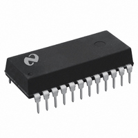
... RSI or out of TSO while CE is active (high). The transfer depends on the logic state of TRB. www.national.com Plastic Dual-In-Line DS012877-2 Top View Order Number TP11362AN See NS Package Number N24A CLK Master clock input. CLK may be asynchronous to PSCK or ASCK. CE Chip enable input. When CE is high, it enables data transfer. ...
Page 3
Pin Descriptions (Continued) QSEL0, QSEL1 ADPCM bit rate select inputs. The QSEL0 and QSE1 signals are strobed in with the falling edge of CE. The QSEL0 and QSEL1 select the conversion bit rate of the PCM data just clocked in ...
Page 4
Functional Description The TP11362A is capable of processing eight independent channels (half duplex) or four full-duplex PCM channels within 125 µs (8 kHz). The logic state of TRB at the falling edge of CE determines which input register is active ...
Page 5
Functional Description (Continued receive (decoder) operation. For the encoding opera- tion, the PCM data is stored in the 8-bit shift register at the falling edge of CE while TRB is high. The TP11362A pro- cesses the data within ...
Page 6
Functional Description www.national.com (Continued) 6 ...
Page 7
Functional Description (Continued) Table 3 shows the position of the ADPCM data in the 5-bit in- put register when five ASCK low going pulses are available while CE is high. Only the last four bits of the ADPCM input register ...
Page 8
Functional Description to the falling edge of CE are latched in. In Table 3 , the last in- put bit prior to to the CE falling edge is the LSB of the AD- PCM data word. Note that the serial ...
Page 9
Functional Description (Continued) G.726. At power up, the outputs TSO and RSO are in TRI-STATE mode. This “cold” reset process is asynchronous and takes approximately 2000 CLK cycles for the initializa- tion. During the reset process, the outputs TSO and ...
Page 10
... Absolute Maximum Ratings TGT: FNXref NS0465*) If Military/Aerospace specified devices are required, please contact the National Semiconductor Sales Office/ Distributors for availability and specifications GND CC Voltage at Any Digital Inputs or Outputs GND − 0. Electrical Characteristics Unless otherwise noted, limits printed in bold characters are guaranteed forV − ...
Page 11
Timing Specifications (Continued) Unless otherwise noted, limits printed in bold characters are guaranteed for V −40˚C to +85˚C by correlation with 100% electrical testing at T production tests and/or product design and characterization. Typical values are specified at V Symbol ...
Page 12
Timing Specifications (Continued) www.national.com 12 ...
Page 13
Applications Information FIGURE 7. Typical Application in an ISDN Pair Gain System 13 DS012877-9 www.national.com ...
Page 14
Applications Information Note 6: The duty cycle of CE can be adjusted to adapt to different PCM data bit clocks of the COMBO. Note 7: The DX data output is shown with the long frame sync mode (non-delayed data timing ...
Page 15
... Physical Dimensions inches (millimeters) unless otherwise noted 24-Lead (0.600" Wide) Molded Dual-In-Line Package Order Number TP11362AN NS Package Number N24A 15 www.national.com ...
Page 16
... Hong Kong Ltd. Fax: +49 (0) 1 80-530 85 86 13th Floor, Straight Block, Email: europe.support@nsc.com Ocean Centre, 5 Canton Rd. Tsimshatsui, Kowloon Tel: +49 (0) 1 80-532 78 32 Hong Kong Tel: (852) 2737-1600 Tel: +49 (0) 1 80-534 16 80 Fax: (852) 2736-9960 National Semiconductor Japan Ltd. Tel: 81-3-5620-6175 Fax: 81-3-5620-6179 ...