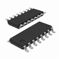
SI3019-KS Silicon Laboratories Inc, SI3019-KS Datasheet - Page 82

SI3019-KS
Manufacturer Part Number
SI3019-KS
Description
IC VOICE DAA GCI/PCM/SPI 16SOIC
Manufacturer
Silicon Laboratories Inc
Type
Chipsetr
Datasheet
1.SI3056-KS.pdf
(96 pages)
Specifications of SI3019-KS
Package / Case
16-SOIC (3.9mm Width)
Function
Data Access Arrangement (DAA)
Interface
GCI, PCM, SPI
Number Of Circuits
1
Voltage - Supply
3 V ~ 3.6 V
Current - Supply
8.5mA
Operating Temperature
0°C ~ 70°C
Mounting Type
Surface Mount
Includes
Line Voltage Monitor, Loop Current Monitor, Overload Detection, Parallel Handset Detection, Polarity Reversal Detection, TIP and
Product
Modem Chip
Supply Voltage (min)
3 V
Supply Current
8.5 mA
Maximum Operating Temperature
+ 70 C
Minimum Operating Temperature
0 C
Mounting Style
SMD/SMT
Lead Free Status / RoHS Status
Contains lead / RoHS non-compliant
Power (watts)
-
Lead Free Status / RoHS Status
Lead free / RoHS Compliant, Contains lead / RoHS non-compliant
Available stocks
Company
Part Number
Manufacturer
Quantity
Price
Part Number:
SI3019-KS
Manufacturer:
SILICON LABS/芯科
Quantity:
20 000
Company:
Part Number:
SI3019-KSR
Manufacturer:
SILICONLAB
Quantity:
2 722
Si3018/19/10
Register 59. Spark Quenching Control
Reset settings = xxxx_xxxx
82
Name
Bit
Type
7
6
5
4
3
2
1
0
Bit
Reserved Always write this bit to zero.
Reserved Always write this bit to zero.
Reserved Always write this bit to zero.
Reserved Always write this bit to zero.
Name
GCE
SQ1
SQ0
RG1
D7
Spark Quenching.
This bit, in combination with the OHS bit (Register 16), and the OHS2 bit (Register 31), sets
the amount of time for the line-side device to go on-hook. The on-hook speeds specified are
measured from the time the OH bit is cleared until loop current equals zero.
OHS
Spark Quenching.
This bit, in combination with the OHS bit (Register 16), and the OHS2 bit (Register 31), sets
the amount of time for the line-side device to go on-hook. The on-hook speeds specified are
measured from the time the OH bit is cleared until loop current equals zero.
OHS
Receive Gain 1 (Line-side Revision E or later).
This bit enables receive path gain adjustment.
0 = No gain applied to hybrid, full scale RX on line = 0 dBm.
1 = 1 dB of gain applied to hybrid, full scale RX on line = –1 dBm.
Guarded Clear Enable (Line-side Revision E or later).
This bit (in conjunction with the R2 bit set to 1), enables the Si3056 to meet BT’s Guarded
Clear Spec (B5 6450, Part 1: 1993, Section 15.4.3.3). With these bits set, the DAA will draw
approximately 2.5 mA of current from the line while on-hook.
0 = default, DAA does not draw loop current.
1 = Guarded Clear enabled, DAA draws 2.5 mA while on-hook to meet Guarded Clear
requirement.
SQ1
R/W
0
0
1
0
0
1
D6
OHS2
OHS2
D5
0
1
X
0
1
X
SQ0
R/W
D4
SQ[1:0]
SQ[1:0]
00
00
11
00
00
11
D3
Rev. 1.03
RG1
R/W
D2
Function
Less than 0.5 ms
3 ms ±10% (meets ETSI standard)
26 ms ±10% (meets Australia spark quenching
spec)
Less than 0.5 ms
3 ms ±10% (meets ETSI standard)
26 ms ±10% (meets Australia spark quenching
spec)
Mean On-Hook Speed
Mean On-Hook Speed
GCE
R/W
D1
D0


