PC16550DN/NOPB National Semiconductor, PC16550DN/NOPB Datasheet - Page 15
PC16550DN/NOPB
Manufacturer Part Number
PC16550DN/NOPB
Description
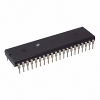
IC UART WITH FIFO 40-DIP
Manufacturer
National Semiconductor
Datasheet
1.PC16550DVNOPB.pdf
(22 pages)
Specifications of PC16550DN/NOPB
Features
Modem Control Function
Number Of Channels
1, UART
Fifo's
16 Byte
Voltage - Supply
4.5 V ~ 5.5 V
With False Start Bit Detection
Yes
With Modem Control
Yes
Mounting Type
Through Hole
Package / Case
40-DIP (0.600", 15.24mm)
Supply Voltage (max)
5.5 V
Supply Voltage (min)
4.5 V
Msl
MSL 1 - Unlimited
Data Rate Max
128Kbps
Ic Function
UART IC
Interface Type
Serial
No. Of Transceivers
1
Peak Reflow Compatible (260 C)
Yes
Supply Current
15mA
Rohs Compliant
Yes
Lead Free Status / RoHS Status
Lead free / RoHS Compliant
Other names
*PC16550DN
*PC16550DN/NOPB
PC16550DN
*PC16550DN/NOPB
PC16550DN
Available stocks
Company
Part Number
Manufacturer
Quantity
Price
Company:

Part Number:
PC16550DN/NOPB
Manufacturer:
NSC
Quantity:
1 011
Company:
Part Number:
PC16550DN/NOPB
Manufacturer:
National
Quantity:
695
Part Number:
PC16550DN/NOPB
Manufacturer:
TI/德州仪器
Quantity:
20 000


Baud Rate
8 0 Registers
The system programmer may access any of the UART reg-
isters summarized in Table II via the CPU These registers
control UART operations including transmission and recep-
tion of data Each register bit in Table II has its name and
reset state shown
8 1 LINE CONTROL REGISTER
The system programmer specifies the format of the asyn-
chronous data communications exchange and set the Divi-
sor Latch Access bit via the Line Control Register (LCR)
The programmer can also read the contents of the Line
Control Register The read capability simplifies system pro-
gramming and eliminates the need for separate storage in
system memory of the line characteristics Table II shows
the contents of the LCR Details on each bit follow
Bits 0 and 1 These two bits specify the number of bits in
each transmitted or received serial character The encoding
of bits 0 and 1 is as follows
Bit 2 This bit specifies the number of Stop bits transmitted
and received in each serial character If bit 2 is a logic 0
one Stop bit is generated in the transmitted data If bit 2 is a
logic 1 when a 5-bit word length is selected via bits 0 and 1
one and a half Stop bits are generated If bit 2 is a logic 1
when either a 6- 7- or 8-bit word length is selected two
Stop bits are generated The Receiver checks the first Stop-
bit only regardless of the number of Stop bits selected
Note For baud rates of 250k 300k 375k 500k 750k and 1 5M using a 24 MHz crystal causes minimal error
128000
19200
38400
56000
134 5
1200
1800
2000
2400
3600
4800
7200
9600
110
150
300
600
50
75
Bit 1
0
0
1
1
Decimal Divisor
for 16
2304
1536
1047
Bit 0
857
768
384
192
96
64
58
48
32
24
16
12
c
6
3
2
0
1
0
1
1 8432 MHz Cystal
Clock
Character Length
Percent Error
5 Bits
6 Bits
7 Bits
8 Bits
0 026
0 058
TABLE III Baud Rates Divisors and Crystals
0 69
2 86
Decimal Divisor
for 16
3840
2560
1745
1428
1280
640
320
160
107
96
80
53
40
27
20
10
c
5
3 072 MHz Crystal
15
Clock
Bit 3 This bit is the Parity Enable bit When bit 3 is a logic 1
a Parity bit is generated (transmit data) or checked (receive
data) between the last data word bit and Stop bit of the
serial data (The Parity bit is used to produce an even or odd
number of 1s when the data word bits and the Parity bit are
summed )
Bit 4 This bit is the Even Parity Select bit When bit 3 is a
logic 1 and bit 4 is a logic 0 an odd number of logic 1s is
transmitted or checked in the data word bits and Parity bit
When bit 3 is a logic 1 and bit 4 is a logic 1 an even number
of logic 1s is transmitted or checked
Bit 5 This bit is the Stick Parity bit When bits 3 4 and 5 are
logic 1 the Parity bit is transmitted and checked as a logic 0
If bits 3 and 5 are 1 and bit 4 is a logic 0 then the Parity bit is
transmitted and checked as a logic 1 If bit 5 is a logic 0
Stick Parity is disabled
Bit 6 This bit is the Break Control bit It causes a break
condition to be transmitted to the receiving UART When it
is set to a logic 1 the serial output (SOUT) is forced to the
Spacing (logic 0) state The break is disabled by setting bit 6
to a logic 0 The Break Control bit acts only on SOUT and
has no effect on the transmitter logic
Note This feature enables the CPU to alert a terminal in a computer com-
1 Load an all 0s pad character in response to THRE
2 Set break after the next THRE
3 Wait for the transmitter to be idle (TEMT
During the break the Transmitter can be used as a character timer to accu-
rately establish the break duration
normal transmission has to be restored
munications system If the following sequence is followed no errone-
ous or extraneous characters will be transmitted because of the
break
Percent Error
0 026
0 034
0 312
0 628
1 23
Decimal Divisor
for 16
23040
15360
10473
8565
7680
3840
1920
920
640
576
480
320
240
160
120
60
30
21
18 432 MHz Crystal
c
9
Clock
e
1) and clear break when
Percent Error
2 04
Related parts for PC16550DN/NOPB
Image
Part Number
Description
Manufacturer
Datasheet
Request
R

Part Number:
Description:
UART IC
Manufacturer:
National Semiconductor
Datasheet:

Part Number:
Description:
National Semiconductor [8-Bit D/A Converter]
Manufacturer:
National Semiconductor
Datasheet:
Part Number:
Description:
National Semiconductor [Media Coprocessor]
Manufacturer:
National Semiconductor
Datasheet:
Part Number:
Description:
Digitally Controlled Tone and Volume Circuit with Stereo Audio Power Amplifier, Microphone Preamp Stage and National 3D Sound
Manufacturer:
National Semiconductor
Datasheet:
Part Number:
Description:
Digitally Controlled Tone and Volume Circuit with Stereo Audio Power Amplifier, Microphone Preamp Stage and National 3D Sound
Manufacturer:
National Semiconductor
Datasheet:
Part Number:
Description:
AC97 Rev 2 Codec with Sample Rate Conversion and National 3D Sound
Manufacturer:
National Semiconductor
Part Number:
Description:
Manufacturer:
National Semiconductor
Datasheet:
Part Number:
Description:
Manufacturer:
National Semiconductor
Datasheet:
Part Number:
Description:
General Purpose, Low Voltage, Low Power, Rail-to-Rail Output Operational Amplifiers
Manufacturer:
National Semiconductor
Datasheet:
Part Number:
Description:
8-bit 20 MSPS flash A/D converter.
Manufacturer:
National Semiconductor
Datasheet:
Part Number:
Description:
Low Noise Quad Operational Amplifier
Manufacturer:
National Semiconductor
Datasheet:
Part Number:
Description:
Quad Differential Line Receivers
Manufacturer:
National Semiconductor
Datasheet:
Part Number:
Description:
Quad High Speed Trapezoidal? Bus Transceiver
Manufacturer:
National Semiconductor
Datasheet:
Part Number:
Description:
Dual Line Receiver
Manufacturer:
National Semiconductor
Datasheet: