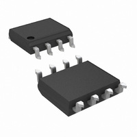
LM4890M/NOPB National Semiconductor, LM4890M/NOPB Datasheet - Page 4

LM4890M/NOPB
Manufacturer Part Number
LM4890M/NOPB
Description
IC AMP AUDIO PWR 1W MONO 8SOIC
Manufacturer
National Semiconductor
Series
Boomer®r
Type
Class ABr
Datasheet
1.LM4890MXNOPB.pdf
(30 pages)
Specifications of LM4890M/NOPB
Output Type
1-Channel (Mono)
Max Output Power X Channels @ Load
1W x 1 @ 8 Ohm
Voltage - Supply
2.2 V ~ 5.5 V
Features
Depop, Shutdown, Thermal Protection
Mounting Type
Surface Mount
Package / Case
8-SOIC (3.9mm Width)
Amplifier Class
AB
No. Of Channels
1
Output Power
1W
Supply Voltage Range
2.2V To 5.5V
Load Impedance
8ohm
Operating Temperature Range
-40°C To +85°C
Amplifier Case Style
SOIC
Rohs Compliant
Yes
For Use With
LM4890MBD - BOARD EVALUATION LM4890M
Lead Free Status / RoHS Status
Lead free / RoHS Compliant
Other names
*LM4890M
*LM4890M/NOPB
LM4890M
*LM4890M/NOPB
LM4890M
www.national.com
I
I
V
V
V
R
P
T
T
THD+N
PSRR
T
I
I
V
V
V
R
T
DD
SD
DD
SD
Symbol
Symbol
WU
SD
SDT
WU
SDIH
SDIL
OS
o
SDIH
SDIL
OS
OUT-GND
OUT-GND
Absolute Maximum Ratings
If Military/Aerospace specified devices are required,
please contact the National Semiconductor Sales Office/
Distributors for availability and specifications.
Electrical Characteristics V
The following specifications apply for the circuit shown in Figure 1 unless otherwise specified. Limits apply for T
Electrical Characteristics V
The following specifications apply for the circuit shown in Figure 1 unless otherwise specified. Limits apply for T
Supply Voltage (Note 11)
Storage Temperature
Input Voltage
Power Dissipation (Note 3)
ESD Susceptibility (Note 4)
Junction Temperature
Thermal Resistance
θ
θ
θ
JC
JA
JA
(SOP)
(SOP)
(8 Bump micro SMD, Note 12)
Quiescent Power Supply Current
Shutdown Current
Shutdown Voltage Input High
Shutdown Voltage Input Low
Output Offset Voltage
Resistor Output to GND (Note 10)
Output Power (8Ω)
Wake-up time
Thermal Shutdown Temperature
Total Harmonic Distortion + Noise
Power Supply Rejection Ratio
(Note 14)
Shut Down Time
Quiescent Power Supply Current
Shutdown Current
Shutdown Voltage Input High
Shutdown Voltage Input Low
Output Offset Voltage
Resistor Output to Gnd (Note 10)
Wake-up time
Parameter
Parameter
−0.3V to V
Internally Limited
−65˚C to +150˚C
DD
DD
V
V
V
THD = 2% (max); f = 1 kHz
P
V
Input Terminated with 10 ohms to
ground
8 Ω load
V
V
V
(Note 2)
IN
IN
SHUTDOWN
o
ripple
IN
IN
SHUTDOWN
= 0.4 Wrms; f = 1kHz
= 5V
= 3V
DD
= 0V, I
= 0V, I
= 0V, I
= 0V, I
150˚C/W
220˚C/W
35˚C/W
= 200mV sine p-p
2000V
150˚C
+0.3V
6.0V
o
o
o
o
Conditions
Conditions
= 0A, No Load
= 0A, 8Ω Load
= 0A, No Load
= 0A, 8Ω Load
= 0V
= 0V
(Notes 1, 2, 8)
(Notes 1, 2, 8)
4
Operating Ratings
Soldering Information
See AN-1112 "microSMD Wafers Level Chip Scale
Package."
See AN-1187 "Leadless Leadframe Package (LLP)."
Temperature Range
Supply Voltage
θ
θ
θ
θ
T
JA
JC
JA
JA
MIN
(9 Bump micro SMD, Note 12)
(MSOP)
(MSOP)
(LLP)
≤ T
A
≤ T
MAX
66 (f = 1kHz)
(Note 6)
(Note 6)
Typical
Typical
217Hz)
62 (f =
170
170
120
0.1
8.5
1.0
0.1
1.0
3.5
4.5
0.1
8.5
4
5
7
7
LM4890
LM4890
(Notes 7, 9)
(Notes 7, 9)
Limit
Limit
220
150
190
180
2.0
1.2
0.4
9.7
7.0
0.8
2.0
1.2
0.4
9.7
7.0
10
50
55
50
8
7
9
−40˚C ≤ T
2.2V ≤ V
A
A
= 25˚C.
= 25˚C.
mA (max)
mA (max)
mV (max)
mA (max)
mA (max)
mV (max)
ms (max)
ms (max)
ms (max)
µA (max)
kΩ (max)
µA (max)
kΩ (max)
DD
˚C (max)
kΩ (min)
dB (min)
kΩ (min)
˚C (min)
(Limits)
V (max)
(Limits)
V (min)
V(max)
180˚C/W
190˚C/W
220˚C/W
A
V(min)
Units
Units
56˚C/W
≤ 85˚C
≤ 5.5V
W
%


