LM4935RL/NOPB National Semiconductor, LM4935RL/NOPB Datasheet
LM4935RL/NOPB
Specifications of LM4935RL/NOPB


Related parts for LM4935RL/NOPB

LM4935RL/NOPB Summary of contents
Page 1
... THD LS_V = 4.2V, 8Ω, 1% THD LS_V = 3.3V, 8Ω, 1% THD LS DD Boomer ® registered trademark of National Semiconductor Corporation. © 2006 National Semiconductor Corporation j Supply Voltage Range BB_V = 1.8V to 4.5V, DD D_V & PLL_V DD LS_V & A_V DD n Shutdown Current n PSRR @ 217 Hz, A_V ...
Page 2
LM4935 Overview www.national.com FIGURE 1. Conceptual Schematic 2 20134101 ...
Page 3
Typical Application FIGURE 2. Example Application in Multimedia Mobile Phone 3 20134102 www.national.com ...
Page 4
General Description ..................................................................................................................................... 1 2.0 Applications .................................................................................................................................................. 1 3.0 Key Specifications ........................................................................................................................................ 1 4.0 Features ....................................................................................................................................................... 1 5.0 LM4935 Overview ........................................................................................................................................ 2 6.0 Typical Application ........................................................................................................................................ 3 7.0 Connection Diagrams ................................................................................................................................... 6 7.1 PIN TYPE DEFINITIONS .......................................................................................................................... 8 8.0 ...
Page 5
LM4935 Demonstration Board Schematic Diagram .............................................................................. 105 15.0 Demoboard PCB Layout ........................................................................................................................ 106 16.0 Product Status Definitions ...................................................................................................................... 111 17.0 Revision History ..................................................................................................................................... 112 18.0 Physical Dimensions .............................................................................................................................. 113 Table of Contents (Continued) 5 www.national.com ...
Page 6
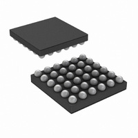
Connection Diagrams 49 Bump micro SMDxt Top View (Bump Side Down) Order Number LM4935RL See NS Package Number RLA49UUA www.national.com 49 Bump micro SMDxt Marking XY — Date Code TT — Die Traceability G — Boomer G7 — LM4935RL ...
Page 7
Connection Diagrams Pin Descriptions Pin Pin Name Type Direction A1 EP_NEG Analog Output A2 A_V Supply Input DD A3 INT_MIC_POS Analog Input A4 EXT_MIC Analog Input A5 VSAR2 Analog Input A6 VSAR1 Analog Input A7 PLL_V Supply Input SS ...
Page 8
Connection Diagrams Pin Descriptions (Continued) Pin Pin Name Type Direction G6 D_V Supply Input SS G7 MCLK Digital Input 7.1 PIN TYPE DEFINITIONS Analog Input — A pin that is used by the analog and is never driven by ...
Page 9
... Absolute Maximum Ratings (Notes Military/Aerospace specified devices are required, please contact the National Semiconductor Sales Office/ Distributors for availability and specifications. Analog Supply Voltage (A_V & LS_V ) DD DD Digital Supply Voltage (BB_V & D_V & PLL_V ) Storage Temperature Power Dissipation (Note 3) ...
Page 10
Electrical Characteristics BB_V = 1.8V, A_V = 3.3V, LS_V DD DD otherwise stated. Limits apply for 25˚C. (Continued) Symbol Parameter DC CURRENT CONSUMPTION DACI DAC Active Current DD SARI SAR Active Current DD LSI Loudspeaker Quiescent Current DD HPI ...
Page 11
Electrical Characteristics BB_V = 1.8V, A_V = 3.3V, LS_V DD DD otherwise stated. Limits apply for 25˚C. (Continued) Symbol Parameter HEADPHONE AMPLIFIER SNR Signal to Noise Ratio HP HP Headphone Harmonic Distortion THD+N e Output Noise N ∆A Stereo ...
Page 12
Electrical Characteristics BB_V = 1.8V, A_V = 3.3V, LS_V DD DD otherwise stated. Limits apply for 25˚C. (Continued) Symbol Parameter STEREO DAC R DAC Ripple DAC PB DAC Passband DAC SBA DAC Stopband Attenuation DAC SNR DAC Signal to ...
Page 13
Electrical Characteristics BB_V = 1.8V, A_V = 3.3V, LS_V DD DD otherwise stated. Limits apply for 25˚C. (Continued) Symbol Parameter VOLUME CONTROL VCR MIC Volume Control Range MIC VCR SIDETONE Volume Control Range SIDE SS AUX VCR Stepsize AUX ...
Page 14
Electrical Characteristics BB_V = 1.8V, A_V = 3.3V, LS_V DD DD otherwise stated. Limits apply for 25˚C. (Continued) Symbol Parameter AUDIO PATH GAIN W/ STEREO (bit 6 of 0x00h) ENABLED (AUX_L & AUX_R signals identical and selected onto mixer) ...
Page 15
Electrical Characteristics BB_V = 1.8V, A_V = 3.3V, LS_V DD DD otherwise stated. Limits apply for 25˚C. (Continued) Symbol Parameter Total DC Power Dissipation MP3 Mode Power Dissipation FM Mode Power Dissipation VOICE CODEC Mode Power Dissipation VOICE Module ...
Page 16
Electrical Characteristics BB_V = 1.8V, A_V = 3.3V, LS_V DD DD otherwise stated. Limits apply for 25˚C. (Continued) Note 1: Absolute Maximum Ratings indicate limits beyond which damage to the device may occur. Operating Ratings indicate conditions for which ...
Page 17
System Control 2 Method Compatible Interface 2 11 SIGNALS mode the LM4935 pin SCL is used for the I signals need a pull-up resistor according 11.2 I ...
Page 18
System Control w = write (SDA = “0” read (SDA = “1”) ack = acknowledge (SDA pulled down by slave repeated start www.national.com (Continued) 2 Example I C Write Cycle 18 201341Q5 ...
Page 19
System Control (Continued) When a READ function accomplished, a WRITE function must precede the READ function, as shown in the Read Cycle waveform TIMING PARAMETERS Symbol 1 Hold Time (repeated) START Condition ...
Page 20
System Control Method 2. SPI/Microwire Control/3–wire Control The LM4935 can be controlled via a three wire interface consisting of a clock, data and an active low chip_select. To use this control method connect SPI_MODE to BB_V If the application ...
Page 21
Status & Control Registers Address Register 7 0x00h BASIC OCL 0x01h CLOCKS 0x02h PLL_M PLLINPUT 0x03h PLL_N 0x04h PLL_P RSVD 0x05h PLL_MOD RSVD 0x06h ADC_1 HPF_MODE 0x07h ADC_2 IF216 0x08h AGC_1 NOISE_GATE_THRESHOLD 0x09h AGC_2 AGC_TIGHT 0x0Ah AGC_3 0x0Bh MIC_1 ...
Page 22
Status & Control Registers 12.1 BASIC CONFIGURATION REGISTER This register is used to control the basic function of the chip. Bits Field 1:0 CHIP_MODE The LM4935 can be placed in one of four modes which dictate its basic operation. ...
Page 23
Status & Control Registers 12.2 CLOCKS CONFIGURATION REGISTER This register is used to control the clocks throughout the chip. Bits Field 0 DAC_CLK Selects the clock to be used by the audio DAC system. 1 ADC_CLK Selects the clock ...
Page 24
Status & Control Registers 12.3 LM4935 CLOCK NETWORK The audio ADC operates at 125*fs requires a 1.000 MHz clock to sample at 8 kHz (at point C as marked on the following diagram). The stereo DAC operates ...
Page 25
Status & Control Registers 12.4 COMMON CLOCK SETTINGS FOR THE DAC & ADC The DAC has an over sampling rate of 125 but requires a 250*fs clock at point B. This allows a simple clocking solution as it will ...
Page 26
Status & Control Registers 12.5 PLL M DIVIDER CONFIGURATION REGISTER This register is used to control the input section of the PLL. Bits Field 0 RSVD RESERVED 6:1 PLL_M 7 PLL_INPUT Programs the PLL input multiplexer to select between: ...
Page 27
Status & Control Registers 12.6 PLL N DIVIDER CONFIGURATION REGISTER This register is used to control the feedback divider of the PLL. Bits Field 7:0 PLL_N Programs the PLL feedback divider as follows: The N divider should be set ...
Page 28
Status & Control Registers 12.7 PLL P DIVIDER CONFIGURATION REGISTER This register is used to control the output divider of the PLL. Bits Field 0 RSVD RESERVED 3:1 PLL_P 6:4 Q_DIV Programs the Q Divider (divides from an expected ...
Page 29
Status & Control Registers 12.8 PLL N MODULUS CONFIGURATION REGISTER This register is used to control the modulation applied to the feedback divider of the PLL. Bits Field 4:0 PLL_N_MOD Programs the PLL N divider’s fractional component: 6:5 DITHER_LEVEL ...
Page 30
Status & Control Registers 12.9 FURTHER NOTES ON PLL PROGRAMMING The sigma-delta PLL is designed to drive audio circuits requiring accurate clock frequencies MHz with frequency errors noise-shaped away from the audio band. The 5 ...
Page 31
Status & Control Registers These tables cover the most common applications, obtaining clocks for derivative sample rates such as 22.05 kHz should be done by increasing the P divider value or using the R/Q dividers. If the user needs ...
Page 32
Status & Control Registers 12.10 ADC_1 CONFIGURATION REGISTER This register is used to control the LM4935’s audio ADC. Bits Field 0 MIC_SELECT If set the microphone preamp output is added to the ADC input signal. 1 CPI_SELECT If set ...
Page 33
Status & Control Registers 12.11 ADC_2 CONFIGURATION REGISTER This register is used to control the LM4935’s audio ADC. Bits Field 0 ULAW/ALAW If COMPAND is set then the data across the PCM interface to the DAC and from the ...
Page 34
Status & Control Registers 12.12 AGC_1 CONFIGURATION REGISTER This register is used to control the LM4935’s Automatic Gain Control. (Note 16) Bits Field 0 AGC_ENABLE If set the AGC controls the analog microphone preamplifier gain into the system. The ...
Page 35
Status & Control Registers 12.13 AGC_2 CONFIGURATION REGISTER This register is used to control the LM4935’s Automatic Gain Control. Bits Field 3:0 AGC_MAX_GAIN This programs the maximum gain that the AGC algorithm can apply to the microphone preamplifier. AGC_MAX_GAIN ...
Page 36
Status & Control Registers 12.14 AGC_3 CONFIGURATION REGISTER This register is used to control the LM4935’s Automatic Gain Control. (Note 18) Bits Field 4:0 AGC_HOLDTIME Programs the amount of delay before the AGC algorithm begins to adjust the gain ...
Page 37
Status & Control Registers 12.15 AGC OVERVIEW The Automatic Gain Control (AGC) system can be used to optimize the dynamic range of the ADC for voice data when the level of the source is unknown. A target level for ...
Page 38
Status & Control Registers 12.16 MIC_1 CONFIGURATION REGISTER This register is used to control the microphone configuration. Bits Field 3:0 PREAMP_GAIN Programs the gain applied to the microphone preamplifier if the AGC is not in use. 4 MIC_MUTE If ...
Page 39
Status & Control Registers 12.17 MIC_2 CONFIGURATION REGISTER This register is used to control the microphone configuration. Bits Field 0 OCL_ Selects the voltage used as virtual ground (HP_VMID pin) in OCL mode. This will depend on the VCM_ ...
Page 40
Status & Control Registers 12.18 SIDETONE ATTENUATION REGISTER This register is used to control the analog sidetone attenuation. (Note 20) Bits Field 3:0 SIDETONE_ Programs the attenuation applied to the microphone preamp output to produce a sidetone signal. ATTEN ...
Page 41
Status & Control Registers 12.19 CP_INPUT CONFIGURATION REGISTER This register is used to control the differential cell phone input. Bits Field 4:0 CPI_LEVEL Programs the gain/attenuation applied to the cell phone input. 5 CPI_MUTE If set the CPI input ...
Page 42
Status & Control Registers 12.20 AUX_LEFT CONFIGURATION REGISTER This register is used to control the left aux analog input. Bits Field 4:0 AUX_ Programs the gain/attenuation applied to the AUX LEFT analog input to the mixer. (Note 21) LEFT_ ...
Page 43
Status & Control Registers 12.21 AUX_RIGHT CONFIGURATION REGISTER This register is used to control the right aux analog input. Bits Field 4:0 AUX_ Programs the gain/attenuation applied to the AUX RIGHT analog input to the mixer. (Note 22) RIGHT_ ...
Page 44
Status & Control Registers 12.22 DAC CONFIGURATION REGISTER This register is used to control the DAC levels to the mixer. Bits Field 4:0 DAC_LEVEL Programs the gain/attenuation applied to the DAC input to the mixer. (Note 23) 00100 to ...
Page 45
Status & Control Registers 12.23 CP_OUTPUT CONFIGURATION REGISTER This register is used to control the differential cell phone output. (Note 24) Bits Field 0 MIC_SELECT If set the microphone channel of the mixer is added to the cellphone output ...
Page 46
Status & Control Registers 12.24 AUX_OUTPUT CONFIGURATION REGISTER This register is used to control the differential auxiliary output. (Note 25) Bits Field 0 CPI_SELECT If set the cell phone input channel of the mixer is added to the aux ...
Page 47
Status & Control Registers 12.25 LS_OUTPUT CONFIGURATION REGISTER This register is used to control the loudspeaker output. (Note 26) Bits Field 0 CPI_SELECT If set the cell phone input channel of the mixer is added to the loudspeaker output ...
Page 48
Status & Control Registers 12.26 HP_OUTPUT CONFIGURATION REGISTER This register is used to control the stereo headphone output. (Note 27) Bits Field 0 SIDETONE_SELECT If set the sidetone channel of the mixer is added to both of the headphone ...
Page 49
Status & Control Registers 12.27 EP_OUTPUT CONFIGURATION REGISTER This register is used to control the mono earpiece output. (Note 28) Bits Field 0 SIDETONE_SELECT If set the sidetone channel of the mixer is added to the earpiece output signal. ...
Page 50
Status & Control Registers 12.28 DETECT CONFIGURATION REGISTER This register is used to control the headset detection system. Bits Field 0 DET_INT If set an IRQ is raised when a change is detected in the headset status. Clearing this ...
Page 51
Status & Control Registers 12.29 HEADSET DETECT OVERVIEW The LM4935 has built in monitors to automatically detect headset insertion or removal. The detection scheme can differentiate between mono, stereo, mono-cellular and stereo-cellular headsets. Upon detection of headset insertion or ...
Page 52
Status & Control Registers FIGURE 8. Headset Configurations Supported by the LM4935 The wiring of the headset jack to the LM4935 will depend on the intended mode of the headphone amplifier: www.national.com (Continued) 52 20134113 ...
Page 53
Status & Control Registers FIGURE 9. Connection of Headset Jack to LM4935 Depends on the Mode of the Headphone Amplifier. (Continued) 53 20134114 www.national.com ...
Page 54
Status & Control Registers 12.30 STATUS REGISTER This register is used to report the status of the device. Bits Field 0 HEADSET This field is high when headset presence is detected (only valid if the detection system is enabled). ...
Page 55
Status & Control Registers 12.31 AUDIO INTERFACE CONFIGURATION REGISTER This register is used to control the configuration of the audio data interfaces. Bits Field 1:0 AUDIO_IF_MODE Selects the function of the 6 audio interface IOs. AUDIO_IF_MODE ...
Page 56
Status & Control Registers 12.32 DIGITAL AUDIO DATA FORMATS I2S master mode can only be used when the DAC is enabled unless the ADC_I2S_M bit is set. PCM Master mode can only be used when the ADC is enabled. ...
Page 57
Status & Control Registers 12.33 GPIO CONFIGURATION REGISTER This register is used to control the GPIO system. Bits Field 2:0 GPIO_SEL This sets the function of the GPIOs when the Audio Interface is not using them. GPIO_SEL Setting GPIO_SEL ...
Page 58
Status & Control Registers 12.34 SAR CHANNELS 0 & 1 CONFIGURATION REGISTER This register is used to control channel 0 and 1 of the SAR system. (Note 31) Bits Field 2:0 SLOT_0_FS 3 SLOT_0_ENB 6:4 SLOT_1_FS 7 SLOT_1_ENB Note ...
Page 59
Status & Control Registers 12.35 SAR CHANNELS 2 & 3 CONFIGURATION REGISTER This register is used to control channel 2 and 3 of the SAR system. (Note 31) Bits Field 2:0 SLOT_2_FS 3 SLOT_2_ENB 4 SLOT_3_ENB 5 SLOT_2_VBB (Continued) ...
Page 60
Status & Control Registers 12.36 SAR DATA REGISTERS These registers are used to read the 8 MSBs from the 4 SAR channels. Bits Field 7:0 SLOT_0_DATA Latest slot 0 sample bits 11:4. Bits Field 7:0 SLOT_1_DATA ...
Page 61
Status & Control Registers 12.37 SAR OVERVIEW The SAR controller works via a scheduler that allocates time slots for each of the four channels. All four channels can operate up to the same maximum frequency. When the sampling frequency ...
Page 62
Status & Control Registers Only the 8 MSBS [11:4] from the 12 bits of SAR output data can be read back using the I The SPI interface can be used to access all 12 bits of the SAR output ...
Page 63
Status & Control Registers 12.38 DC VOLUME CONFIGURATION REGISTER This register is used to control the DC volume control system. Bits Field 0 DC_VOL_ENB 1 DC_VOL_EFFECT 3:2 MAX_LEVEL Note 32: The correlation between the voltage on VSAR1 to the ...
Page 64
Status & Control Registers 12.39 SAR TRIGGER 1 CONFIGURATION REGISTER This register is used to setup a voltage trigger on one of the SAR outputs. Bits Field 0 TRIG_1_ENB 1 TRIG_1_DIR 3:2 TRIG_1_SOURCE 7:4 TRIG_1_LSB www.national.com (Continued) TABLE 40. ...
Page 65
Status & Control Registers 12.40 SAR TRIGGER 1 MSBs CONFIGURATION REGISTER This register is used to setup the threshold of a voltage trigger on one of the SAR outputs. Bits Field 7:0 TRIG_1_MSB Sets bits 11:4 of the threshold ...
Page 66
Status & Control Registers 12.41 SAR TRIGGER 2 CONFIGURATION REGISTER This register is used to setup a voltage trigger on one of the SAR outputs. Bits Field 0 TRIG_2_ENB 1 TRIG_2_DIR 3:2 TRIG_2_SOURCE 7:4 TRIG_2_LSB www.national.com (Continued) TABLE 42. ...
Page 67
Status & Control Registers 12.42 SAR TRIGGER 2 MSBs CONFIGURATION REGISTER This register is used to setup the threshold of a voltage trigger on one of the SAR outputs. Bits Field 7:0 TRIG_2_MSB Sets bits 11:4 of the threshold ...
Page 68
Status & Control Registers 12.43 DEBUG REGISTER This register is used to set test modes within the device. Bits Field 0 RSVD Reserved 1 RSVD Reserved 2 RSVD Reserved 3 SOFT_RESET This field can be used to reset the ...
Page 69
Typical Performance Characteristics (For all performance curves AV refers to the voltage applied to the A_V DD to the D_V and PLL_V pins Stereo DAC Frequency Response f = 8kHz S Stereo DAC Frequency Response ...
Page 70
Typical Performance Characteristics Stereo DAC Frequency Response f = 32kHz S Stereo DAC Frequency Response f = 48kHz S THD+N vs Stereo DAC Input Voltage (0dB DAC, AUXOUT) www.national.com (Continued) Stereo DAC Frequency Response Zoom 20134142 Stereo DAC Frequency ...
Page 71
Typical Performance Characteristics MONO ADC Frequency Response f = 8kHz, 6dB MIC S MONO ADC Frequency Response f = 8kHz, 36dB MIC S MONO ADC Frequency Response f = 16kHz, 6dB MIC S (Continued) MONO ADC Frequency Response Zoom ...
Page 72
Typical Performance Characteristics MONO ADC Frequency Response f = 16kHz, 36dB MIC S MONO ADC Frequency Response f = 24kHz, 6dB MIC S MONO ADC Frequency Response f = 24kHz, 36dB MIC S www.national.com (Continued) MONO ADC Frequency Response ...
Page 73
Typical Performance Characteristics MONO ADC Frequency Response f = 32kHz, 6dB MIC S MONO ADC Frequency Response f = 32kHz, 36dB MIC S MONO ADC HPF Frequency Response f = 8kHz, 36dB MIC S (from left to right: HPF_MODE ...
Page 74
Typical Performance Characteristics MONO ADC HPF Frequency Response f = 24kHz, 36dB MIC S (from left to right: HPF_MODE ’00’, ’10’, ’01’) MONO ADC THD+N vs MIC Input Voltage (f = 8kHz, 6dB MIC) S MONO ADC PSRR vs ...
Page 75
Typical Performance Characteristics MONO ADC PSRR vs Frequency AV = 3.3V, 36dB MIC DD AUXOUT PSRR vs Frequency AV = 3.3V, 0dB AUX DD (AUX inputs terminated) AUXOUT PSRR vs Frequency AV = 3.3V, 0dB CPI DD (CPI inputs ...
Page 76
Typical Performance Characteristics AUXOUT PSRR vs Frequency AV = 3.3V, 0dB DAC DD (DAC inputs selected) CPOUT PSRR vs Frequency AV = 3.3V, 0dB AUX DD (AUX inputs terminated) CPOUT PSRR vs Frequency AV = 3.3V, 0dB DAC DD ...
Page 77
Typical Performance Characteristics CPOUT PSRR vs Frequency AV = 3.3V, 36dB MIC DD (EXTMIC inputs terminated, AGC on) CPOUT PSRR vs Frequency AV = 3.3V, 36dB MIC, MICBIAS = 2.0V DD (INTMIC DIFF inputs terminated, AGC off) CPOUT PSRR ...
Page 78
Typical Performance Characteristics CPOUT PSRR vs Frequency AV = 3.3V, 36dB MIC, MICBIAS = 2.8V DD (INTMIC DIFF inputs terminated, AGC off) CPOUT PSRR vs Frequency AV = 5V, 36dB MIC, MICBIAS = 2.0V DD (INTMIC DIFF inputs terminated, ...
Page 79
Typical Performance Characteristics CPOUT PSRR vs Frequency AV = 5V, 36dB MIC, MICBIAS = 2.8V DD (INTMIC DIFF inputs terminated, AGC off) CPOUT PSRR vs Frequency AV = 5V, 36dB MIC, MICBIAS = 3.3V DD (INTMIC DIFF inputs terminated, ...
Page 80
Typical Performance Characteristics Earpiece PSRR vs Frequency AV = 3.3V, 0dB AUX DD (AUX inputs terminated) Earpiece PSRR vs Frequency AV = 3.3V, 0dB CPI DD (CPI input terminated) Earpiece PSRR vs Frequency AV = 3.3V, 0dB DAC DD ...
Page 81
Typical Performance Characteristics Headphone PSRR vs Frequency AV = 3.3V, 0dB AUX, OCL 1.2V DD (AUX inputs terminated) Headphone PSRR vs Frequency AV = 3.3V, 0dB CPI, OCL 1.2V DD (CPI input terminated) Headphone PSRR vs Frequency AV = ...
Page 82
Typical Performance Characteristics Headphone PSRR vs Frequency AV = 3.3V, 0dB AUX, OCL 1.5V DD (AUX inputs terminated) Headphone PSRR vs Frequency AV = 3.3V, 0dB CPI, OCL 1.5V DD (CPI input terminated) Headphone PSRR vs Frequency AV = ...
Page 83
Typical Performance Characteristics Headphone PSRR vs Frequency AV = 3.3V, 0dB AUX (AUX inputs terminated) Headphone PSRR vs Frequency AV = 3.3V, 0dB CPI (CPI input terminated) Headphone PSRR vs Frequency AV = 3.3V, 0dB ...
Page 84
Typical Performance Characteristics Loudspeaker PSRR vs Frequency AV = 3.3V, 0dB AUX DD (AUX inputs terminated) Loudspeaker PSRR vs Frequency AV = 3.3V, 0dB CPI DD (CPI input terminated) Loudspeaker PSRR vs Frequency AV = 3.3V, 0dB DAC DD ...
Page 85
Typical Performance Characteristics INT/EXT MICBIAS PSRR vs Frequency AV = 3.3V, MICBIAS = 2.0V DD INT/EXT MICBIAS PSRR vs Frequency AV = 3.3V, MICBIAS = 2.5V DD INT/EXT MICBIAS PSRR vs Frequency AV = 3.3V, MICBIAS = 2.8V DD ...
Page 86
Typical Performance Characteristics INT/EXT MICBIAS PSRR vs Frequency AV = 5V, MICBIAS = 3.3V DD AUXOUT THD+N vs Frequency AV = 5V, 0dB OUT CPOUT THD+N vs Frequency AV = 5V, 0dB ...
Page 87
Typical Performance Characteristics Earpiece THD+N vs Frequency AV = 5V, 0dB 50mW, 32Ω DD OUT Headphone THD+N vs Frequency AV = 5V, OCL 1.5V, 0dB 10mW, 32Ω OUT Headphone THD+N vs Frequency AV = ...
Page 88
Typical Performance Characteristics Headphone THD+N vs Frequency AV = 5V, SE, 0dB 10mW, 32Ω OUT Loudspeaker THD+N vs Frequency 400mW DD OUT 15µH+8Ω+15µH Earpiece THD+N vs Output Power AV = 5V, ...
Page 89
Typical Performance Characteristics Earpiece THD+N vs Output Power AV = 5V, 0dB AUX 1kHz, 32Ω OUT Earpiece THD+N vs Output Power AV = 5V, 0dB CPI 1kHz, 16Ω OUT Earpiece THD+N vs Output ...
Page 90
Typical Performance Characteristics Headphone THD+N vs Output Power AV = 5V, OCL 1.2V, 0dB DAC 1kHz, 16Ω OUT Headphone THD+N vs Output Power AV = 5V, OCL 1.2V, 0dB DAC 1kHz, 32Ω OUT ...
Page 91
Typical Performance Characteristics Headphone THD+N vs Output Power AV = 5V, OCL 1.2V, 12dB DAC 1kHz, 32Ω OUT Headphone THD+N vs Output Power AV = 5V, OCL 1.5V, 0dB DAC 1kHz, 16Ω OUT ...
Page 92
Typical Performance Characteristics Headphone THD+N vs Output Power AV = 5V, OCL 1.5V, 12dB DAC 1kHz, 16Ω OUT Headphone THD+N vs Output Power AV = 5V, OCL 1.5V, 12dB DAC 1kHz, 32Ω OUT ...
Page 93
Typical Performance Characteristics Headphone THD+N vs Output Power AV = 5V, SE, 0dB DAC 1kHz, 32Ω OUT Headphone THD+N vs Output Power AV = 5V, SE, 12dB DAC 1kHz, 16Ω OUT Headphone THD+N ...
Page 94
Typical Performance Characteristics Headphone THD+N vs Output Power AV = 3.3V, OCL 1.2V, 12dB AUX 1kHz, 16Ω OUT Headphone THD+N vs Output Power AV = 5V, OCL 1.2V, 12dB AUX 1kHz, 16Ω OUT ...
Page 95
Typical Performance Characteristics Headphone THD+N vs Output Power AV = 5V, OCL 1.2V, 12dB AUX 1kHz, 32Ω OUT Headphone THD+N vs Output Power AV = 5V, OCL 1.2V, 0dB CPI 1kHz, 16Ω OUT ...
Page 96
Typical Performance Characteristics Headphone THD+N vs Output Power AV = 3.3V, OCL 1.5V, 12dB AUX 1kHz, 16Ω OUT Headphone THD+N vs Output Power AV = 5V, OCL 1.5V, 12dB AUX 1kHz, 16Ω OUT ...
Page 97
Typical Performance Characteristics Headphone THD+N vs Output Power AV = 5V, OCL 1.5V, 12dB AUX 1kHz, 32Ω OUT Headphone THD+N vs Output Power AV = 5V, OCL 1.5V, 0dB CPI 1kHz, 16Ω OUT ...
Page 98
Typical Performance Characteristics Headphone THD+N vs Output Power AV = 5V, SE, 0dB AUX 1kHz, 16Ω OUT Headphone THD+N vs Output Power AV = 5V, SE, 0dB AUX 1kHz, 32Ω OUT Headphone THD+N ...
Page 99
Typical Performance Characteristics Headphone THD+N vs Output Power AV = 5V, SE, 0dB CPI 1kHz, 32Ω OUT Loudspeaker THD+N vs Output Power AV = 4.2V, 0dB AUX 1kHz, 15µH+8Ω+15µH OUT Loudspeaker THD+N vs ...
Page 100
Typical Performance Characteristics Loudspeaker THD+N vs Output Power AV = 5V, 0dB CPI 1kHz, 15µH+8Ω+15µH OUT Loudspeaker THD+N vs Output Power AV = 4.2V, 0dB DAC 1kHz, 15µH+8Ω+15µH OUT AUXOUT THD+N vs Output ...
Page 101
Typical Performance Characteristics AUXOUT THD+N vs Output Voltage AV = 3.3V, 0dB CPI 1kHz, 5kΩ OUT AUXOUT THD+N vs Output Voltage AV = 3.3V, 0dB DAC 1kHz, 5kΩ OUT AUXOUT THD+N vs Output ...
Page 102
Typical Performance Characteristics CPOUT THD+N vs Output Voltage AV = 3.3V, 0dB AUX 1kHz, 5kΩ OUT CPOUT THD+N vs Output Voltage AV = 3.3V, 0dB DAC 1kHz, 5kΩ OUT CPOUT THD+N vs Output ...
Page 103
Typical Performance Characteristics CPOUT THD+N vs Output Voltage AV = 3.3V, 12dB DAC 1kHz, 5kΩ OUT CPOUT THD+N vs Output Voltage AV = 3.3V, 36dB MIC 1kHz, 5kΩ OUT Headphone Crosstalk vs Frequency ...
Page 104
Typical Performance Characteristics Headphone Crosstalk vs Frequency SE, 0dB AUX, 32Ω www.national.com (Continued) 201341N0 104 ...
Page 105
105 www.national.com ...
Page 106
Demoboard PCB Layout www.national.com Top Silkscreen 106 20134132 ...
Page 107
Demoboard PCB Layout (Continued) Top Layer 107 20134131 www.national.com ...
Page 108
Demoboard PCB Layout www.national.com (Continued) Mid Layer 1 108 20134129 ...
Page 109
Demoboard PCB Layout (Continued) Mid Layer 2 109 20134130 www.national.com ...
Page 110
Demoboard PCB Layout www.national.com (Continued) Bottom Layer 110 20134128 ...
Page 111
... Not in Production National Semiconductor B.V reserves the right to make changes without notice to any products herein to improve reliability, function or design. National does not assume any liability arising out of the application or use of any product or circuit described herein; neither does it convey any license under its patent rights, nor the right of others ...
Page 112
Revision History Rev 1.0 1.1 1.2 1.3 1.4 1.5 1.6 1.7 1.8 1.9 2.0 2.1 2.2 2.3 2.4 www.national.com Date 5/11/05 Filled in the actual limits (for TBDs) under Limit and edited few Typical values, all under the EC ...
Page 113
... BANNED SUBSTANCE COMPLIANCE National Semiconductor manufactures products and uses packing materials that meet the provisions of the Customer Products Stewardship Specification (CSP-9-111C2) and the Banned Substances and Materials of Interest Specification (CSP-9-111S2) and contain no ‘‘Banned Substances’’ as defined in CSP-9-111S2. ...