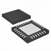
MAX9730ETI+ Maxim Integrated Products, MAX9730ETI+ Datasheet - Page 3

MAX9730ETI+
Manufacturer Part Number
MAX9730ETI+
Description
IC AMP AUDIO PWR 2.4W G 28TQFN
Manufacturer
Maxim Integrated Products
Type
Class Gr
Datasheet
1.MAX9730ETI.pdf
(12 pages)
Specifications of MAX9730ETI+
Output Type
1-Channel (Mono)
Max Output Power X Channels @ Load
2.4W x 1 @ 8 Ohm
Voltage - Supply
2.7 V ~ 5.5 V
Features
Depop, Differential Inputs, Shutdown
Mounting Type
Surface Mount
Package / Case
28-TQFN Exposed Pad
Product
Class-G
Output Power
2.4 W
Common Mode Rejection Ratio (min)
68 dB
Thd Plus Noise
0.12 %
Supply Current
8 mA
Maximum Power Dissipation
1667 mW
Maximum Operating Temperature
+ 85 C
Mounting Style
SMD/SMT
Audio Load Resistance
8 Ohms
Minimum Operating Temperature
- 40 C
Amplifier Class
G
No. Of Channels
1
Supply Voltage Range
2.7V To 5.5V
Load Impedance
8ohm
Operating Temperature Range
-40°C To +85°C
Amplifier Case Style
TQFN
Rohs Compliant
Yes
Lead Free Status / RoHS Status
Lead free / RoHS Compliant
ELECTRICAL CHARACTERISTICS (continued)
(V
10µF; speaker load resistors (R
wise noted. Typical values are at T
Note 1:
Note 2:
Note 3:
Note 4:
Note 5:
Note 6:
Note 7:
Note 8:
Note 9:
Voltage Gain
Continuous Output Power
Output Voltage
Power-Supply Rejection Ratio
(Note 4)
Total Harmonic Distortion Plus
Noise
Signal-to-Noise Ratio
Dynamic Range
CC
= V
2.4W, Single-Supply, Class G Power Amplifier
CPVDD
PARAMETER
All devices are 100% production tested at room temperature. All temperature limits are guaranteed by design.
Testing performed with resistive and inductive loads to simulate an actual speaker load. For dynamic speakers,
R
Designed for 1.8V logic.
R
Amplifier inputs AC-coupled to GND.
Testing performed at room temperature with 8Ω resistive load in series with 68µH inductive load connected across BTL
output for speaker amplifier. Mode transitions are controlled by SHDN. V
Voltage gain is defined as: [V
Mode A tone burst tested at full amplitude for one cycle and half amplitude for nine cycles. Mode B tone burst tested at
full amplitude for three cycles and half amplitude for seven cycles. Full amplitude is defined as 1% THD+N at full battery
(V
5% for three cycles (Mode B).
Dynamic range is calculated by measuring the RMS voltage difference between a -60dBFS output signal and the noise
floor, then adding 60dB. Full scale is defined as the output signal needed to achieve 1% THD+N.
L
IN_
CC
= 8Ω, 68µH.
and R
= 4.2V). Electrical Characteristics table targets must be met at THD+N = 1% for one cycle (Mode A) and THD+N <
= V
SHDN
_______________________________________________________________________________________
FB_
have 0.5% tolerance.
= 3.6V, V
L
) are terminated between OUT+ and OUT-, unless otherwise stated; T
A
GND
= +25°C.) (Notes 1, 2)
SYMBOL
THD+N
PSRR
P
V
SNR
OUT+
DR
= V
A
OUT
OUT
V
CPGND
- V
OUT-
(Notes 4, 7)
THD+N = 1%, f = 1kHz,
R
f = 1kHz, 1% THD+N,
Z
f = 10kHz, 1% THD+N,
Z
V
f = 217Hz, 200mV
f = 1kHz, 200mV
f = 20kHz, 200mV
R
R
V
A-weighted
(Note 9)
L
L
L
CC
L
L
OUT
= 0V, R
= 1µF + 10Ω
= 1µF + 10Ω
= 8Ω
= 8Ω, V
= 8Ω, V
] / [V
= 2.7V to 5.5V
= 0.5V
IN+
IN+
OUT
OUT
- V
RMS
= R
IN-
CONDITIONS
= 1kHz / 400mV
= 1kHz / 1V
P-P
, inputs to GND by C1N,
IN-
].
P-P
P-P
ripple
= 10kΩ, R
ripple
ripple
V
V
V
V
V
V
V
V
V
V
V
V
22Hz to 22kHz
A-weighted
RMS
CC
CC
CC
CC
CC
CC
CC
CC
CC
CC
CC
CC
= 5V
= 4.2V
= 3.6V
= 3.0V
= 5V
= 4.2V
= 3.6V
= 3.0V
= 5V
= 4.2V
= 3.6V
= 3.0V
FB+
RMS
CP
= R
is the peak output transient expressed in dBV.
FB-
= 10kΩ, R
11.5
MIN
63
A
FS
= T
= 100kΩ, C1 = 4.7µF, C2 =
0.007
TYP
1.67
1.25
0.12
MIN
2.4
0.8
7.1
5.9
5.1
4.2
6.5
5.4
4.7
3.8
12
77
77
77
58
95
96
99
to T
MAX
MAX
12.5
, unless other-
UNITS
V
dB
dB
dB
dB
RMS
W
%
3


