TDA2009A STMicroelectronics, TDA2009A Datasheet - Page 9
TDA2009A
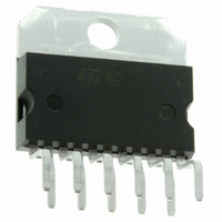
Manufacturer Part Number
TDA2009A
Description
IC AMP AUDIO 12.5W MULTIWATT11
Manufacturer
STMicroelectronics
Type
Class ABr
Datasheet
1.TDA2009A.pdf
(12 pages)
Specifications of TDA2009A
Output Type
2-Channel (Stereo)
Max Output Power X Channels @ Load
12.5W x 2 @ 4 Ohm
Voltage - Supply
8 V ~ 28 V
Features
Short-Circuit and Thermal Protection
Mounting Type
Through Hole
Package / Case
Multiwatt-11 (Vertical, Bent and Staggered Leads)
Amplifier Class
AB
No. Of Channels
2
Output Power
12.5W
Supply Voltage Range
8V To 28V
Load Impedance
4ohm
Operating Temperature Range
-50°C To +150°C
Amplifier Case Style
Multiwatt11
Rohs Compliant
Yes
Lead Free Status / RoHS Status
Lead free / RoHS Compliant
Other names
497-2164-5
Available stocks
Company
Part Number
Manufacturer
Quantity
Price

Part Number:
TDA2009A
Manufacturer:
ST
Quantity:
20 000


APPLICATION SUGGESTION
Figure 17 : P.C. BOARD and Components Layout of the Circuit of Figure 16 (1:1 scale)
(1) The closed loop gain must be higher than 26dB.
BUILD-IN PROTECTION SYSTEMS
THERMAL SHUT-DOWN
The presence of a thermal limiting circuit offers the
following advantages:
1) an averload on the output (even if it is
2) the heatsink can have a smaller factor of safety
The recommended values of the components are those shown on application circuit of fig. 1. Different
values can be used ; the following table can help the designer.
Component
C10, C11
perma nen t ), or an excessi ve ambient
temperature can be easily withstood.
compared with that of a conventional circuit.
There is no device damage in the case of
excessive junction temperature : all that
happens is that P
reduced.
R1, R3
R2, R4
R5, R6
C1, C2
C6, C7
C8, C9
C3
Recommended
1000 F to
2200 F
220 F
1.2k
Value
2.2 F
0.1 F
18k
22 F
o
1
(and therefore P
Input DC Decoupling High Turn-on Delay
Ripple Rejection
Feedback Input DC
Decoupling
Frenquency Stability
Output DC
Decoupling
Close Loop Gain
Setting (1)
Frequency Stability
Purpose
tot
) and I
o
are
Increase of Gain
Decrease of Gain
Danger of Oscillation at High
Frequency with Inductive Load
Better SVR. Increase of the
Switch-on Time
The maximum allowable power dissipation de-
pends upon the size of the external heatsink (i.e.
its thermal resistance); Figure 18 shows this dissi-
pable power as a function of ambient temperature
for different thermal resistance.
Short circuit (AC Conditions). The TDA2009A can
withstand an accidental short circuit from the output
and ground made by a wrong connection during
normal play operation.
Larger than
Decrease of Gain
Increase of Gain
High Turn-on Pop.
Higher Low Frequency
Cut-off. Increase of Noise
Degradation of SVR
Danger of Oscillation
Higher Low-frequency
Cut-off
Smaller than
TDA2009A
9/12
Related parts for TDA2009A
Image
Part Number
Description
Manufacturer
Datasheet
Request
R

Part Number:
Description:
STMicroelectronics [RIPPLE-CARRY BINARY COUNTER/DIVIDERS]
Manufacturer:
STMicroelectronics
Datasheet:
Part Number:
Description:
STMicroelectronics [LIQUID-CRYSTAL DISPLAY DRIVERS]
Manufacturer:
STMicroelectronics
Datasheet:

Part Number:
Description:
BOARD EVAL FOR MEMS SENSORS
Manufacturer:
STMicroelectronics
Datasheet:
Part Number:
Description:
NPN TRANSISTOR POWER MODULE
Manufacturer:
STMicroelectronics
Datasheet:
Part Number:
Description:
TURBOSWITCH ULTRA-FAST HIGH VOLTAGE DIODE
Manufacturer:
STMicroelectronics
Datasheet:
Part Number:
Description:
Manufacturer:
STMicroelectronics
Datasheet:
Part Number:
Description:
DIODE / SCR MODULE
Manufacturer:
STMicroelectronics
Datasheet:
Part Number:
Description:
DIODE / SCR MODULE
Manufacturer:
STMicroelectronics
Datasheet:
Part Number:
Description:
Search -----> STE16N100
Manufacturer:
STMicroelectronics
Datasheet:
Part Number:
Description:
Search ---> STE53NA50
Manufacturer:
STMicroelectronics
Datasheet:
Part Number:
Description:
NPN Transistor Power Module
Manufacturer:
STMicroelectronics
Datasheet:
Part Number:
Description:
DIODE / SCR MODULE
Manufacturer:
STMicroelectronics
Datasheet: