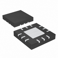
MAX9728AETC+ Maxim Integrated Products, MAX9728AETC+ Datasheet - Page 8

MAX9728AETC+
Manufacturer Part Number
MAX9728AETC+
Description
IC AMP AUDIO .06W STER AB 12TQFN
Manufacturer
Maxim Integrated Products
Series
DirectDrive™r
Type
Class ABr
Datasheet
1.MAX9728AETC.pdf
(19 pages)
Specifications of MAX9728AETC+
Output Type
Headphones, 2-Channel (Stereo)
Max Output Power X Channels @ Load
60mW x 2 @ 32 Ohm
Voltage - Supply
4.5 V ~ 5.5 V
Features
Depop, Short-Circuit and Thermal Protection, Shutdown
Mounting Type
Surface Mount
Package / Case
12-TQFN Exposed Pad
Product
General Purpose Audio Amplifiers
Output Power
60 mW
Thd Plus Noise
0.02 %
Operating Supply Voltage
4.5 V to 5.5 V
Supply Current
3.5 mA
Maximum Power Dissipation
1177 mW
Maximum Operating Temperature
+ 85 C
Mounting Style
SMD/SMT
Minimum Operating Temperature
- 40 C
Supply Voltage (max)
5.5 V
Supply Voltage (min)
4.5 V
Amplifier Class
AB
No. Of Channels
2
Supply Voltage Range
4.5V To 5.5V
Load Impedance
32ohm
Operating Temperature Range
-40°C To +85°C
Amplifier Case Style
TQFN
Rohs Compliant
Yes
Lead Free Status / RoHS Status
Lead free / RoHS Compliant
Since the MAX9728A/MAX9728B do not require output-
coupling capacitors, this problem does not arise.
Additionally, the MAX9728A/MAX9728B feature exten-
sive click-and-pop suppression that eliminates any
audible transient sources internal to the device.
Typically, the output of the device driving the
MAX9728A/MAX9728B has a DC bias of half the supply
voltage. At startup, the input-coupling capacitor is
charged to the preamplifier’s DC-bias voltage through
the input and feedback resistors of the MAX9728A/
MAX9728B, resulting in a DC shift across the capacitor
and an audible click/pop. Delay the rise of SHDN 4 to 5
time constants based on R
startup of the preamplifier, to eliminate clicks-and-pops
caused by the input filter.
The MAX9728A/MAX9728B feature a < 0.1µA, low-
power shutdown mode that reduces quiescent current
consumption and extends battery life for portable appli-
cations. Drive SHDN low to disable the amplifiers and
the charge pump. In shutdown mode, the amplifier out-
put impedance is set to 14kΩ||R
MAX9728B). The amplifiers and charge pump are
enabled once SHDN is driven high.
Under normal operating conditions, linear power ampli-
fiers can dissipate a significant amount of power. The
maximum power dissipation for each package is given
in the Absolute Maximum Ratings section under
Continuous Power Dissipation or can be calculated by
the following equation:
where T
ture, and θ
°C/W as specified in the Absolute Maximum Ratings
section. For example, θ
+68°C/W, and +110°C/W for the TSSOP package.
The MAX9728A/MAX9728B have two power dissipation
sources: a charge pump and the two output amplifiers.
If power dissipation for a given application exceeds the
maximum allowed for a particular package, reduce
V
temperature, or add heatsinking to the device. Large
60mW, DirectDrive, Stereo Headphone
Amplifiers with Shutdown
8
DD
_______________________________________________________________________________________
, increase load impedance, decrease the ambient
J(MAX)
JA
P
DISSPKG MAX
is the reciprocal of the derating factor in
is +150°C, T
Applications Information
(
JA
)
of the Thin QFN package is
=
IN
A
T
is the ambient tempera-
J MAX
and C
(
Power Dissipation
F
θ
JA
(R
)
IN
−
F
T
, relative to the
is 30kΩ for the
A
Shutdown
output, supply, and ground traces decrease θ
ing more heat to be transferred from the package to the
surrounding air.
Thermal-overload protection limits total power dissipa-
tion in the MAX9728A/MAX9728B. When the junction
temperature exceeds +150°C, the thermal-protection
circuitry disables the amplifier output stage. The ampli-
fiers are enabled once the junction temperature cools
by approximately 12°C. This results in a pulsing output
under continuous thermal-overload conditions.
Dynamic range is the difference between the noise floor
of the system and the output level at 1% THD+N.
Determine the system’s dynamic range before setting
the maximum output gain. Output clipping occurs if the
output signal is greater than the dynamic range of the
system. The DirectDrive architecture of the MAX9728A/
MAX9728B has increased the dynamic range compared
to other single-supply amplifiers.
Internal device structures limit the maximum voltage
swing of the MAX9728A/MAX9728B. The output must
not be driven such that the peak output voltage exceeds
the opposite supply voltage by 9V. For example, if V
= 5V, the charge pump sets PV
peak output swing must be less than ±4V to prevent
exceeding the absolute maximum ratings.
The input capacitor (C
resistor (R
DC bias from an incoming signal (see the Functional
Diagram/Typical Operating Circuits ). The AC-coupling
capacitor allows the device to bias the signal to an
optimum DC level. Assuming zero-source impedance,
the -3dB point of the highpass filter is given by:
Choose the C
frequency of interest. Setting f
device’s low-frequency response. Use capacitors
whose dielectrics have low-voltage coefficients, such
as tantalum or aluminum electrolytic. Capacitors with
high-voltage coefficients, such as ceramics, can result
in increased distortion at low frequencies.
IN
), forms a highpass filter that removes the
IN
such that f
f
−
3
dB
IN
=
Maximum Output Swing
), in conjunction with the input
Output Dynamic Range
2π
-3dB
Component Selection
Input-Coupling Capacitor
R C
IN IN
1
-3dB
SS
is well below the lowest
= -5V. Therefore, the
too high affects the
JA
, allow-
DD


