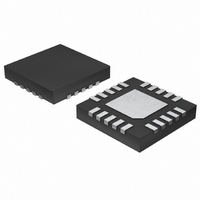
MAX4409ETP+ Maxim Integrated Products, MAX4409ETP+ Datasheet - Page 13

MAX4409ETP+
Manufacturer Part Number
MAX4409ETP+
Description
IC AMP AUDIO .08W STER AB 20TQFN
Manufacturer
Maxim Integrated Products
Series
DirectDrive™r
Type
Class ABr
Datasheet
1.MAX4409ETP.pdf
(20 pages)
Specifications of MAX4409ETP+
Output Type
Headphones, 2-Channel (Stereo)
Max Output Power X Channels @ Load
80mW x 2 @ 16 Ohm
Voltage - Supply
1.8 V ~ 3.6 V
Features
Depop, Short-Circuit and Thermal Protection, Shutdown
Mounting Type
Surface Mount
Package / Case
20-TQFN Exposed Pad
Product
General Purpose Audio Amplifiers
Output Power
80 mW
Common Mode Rejection Ratio (min)
96 dB
Thd Plus Noise
0.002 %
Operating Supply Voltage
1.8 V to 3.6 V
Supply Current
5 mA
Maximum Power Dissipation
2051 mW
Maximum Operating Temperature
+ 85 C
Mounting Style
SMD/SMT
Input Bias Current (max)
0 nA
Input Offset Voltage
0.5 mV
Input Signal Type
Differential
Minimum Operating Temperature
- 40 C
Supply Voltage (max)
3.6 V
Supply Voltage (min)
1.8 V
Amplifier Class
AB
No. Of Channels
2
Supply Voltage Range
1.8V To 3.6V
Load Impedance
16ohm
Operating Temperature Range
-40°C To +85°C
Amplifier Case Style
TQFN
Rohs Compliant
Yes
Lead Free Status / RoHS Status
Lead free / RoHS Compliant
Table 1. Suggested Capacitor Manufacturers
Note: Please indicate you are using the MAX4409 when contacting these component suppliers.
Choose R
tion. Choose the C
lowest frequency of interest. Setting f
affects the low-frequency response of the amplifier. Use
capacitors whose dielectrics have low-voltage coeffi-
cients, such as tantalum or aluminum electrolytic.
Capacitors with high-voltage coefficients, such as
ceramics, may result in increased distortion at low fre-
quencies.
Use capacitors with an ESR less than 100mΩ for opti-
mum performance. Low-ESR ceramic capacitors mini-
mize the output resistance of the charge pump. For
best performance over the extended temperature
range, select capacitors with an X7R dielectric. Table 1
lists suggested manufacturers.
The value of the flying capacitor (C1) affects the load
regulation and output resistance of the charge pump. A
C1 value that is too small degrades the device’s ability
to provide sufficient current drive, which leads to a loss
of output voltage. Increasing the value of C1 improves
load regulation and reduces the charge-pump output
resistance to an extent. See the Output Power vs.
Charge-Pump Capacitance and Load Resistance
graph in the Typical Operating Characteristics. Above
2.2µF, the on-resistance of the switches and the ESR of
C1 and C2 dominate.
The output capacitor value and ESR directly affect the
ripple at PV
put ripple. Likewise, decreasing the ESR of C2 reduces
both ripple and output resistance. Lower capacitance
values can be used in systems with low maximum out-
put power levels. See the Output Power vs. Charge-
Pump Capacitance and Load Resistance graph in the
Typical Operating Characteristics.
The power-supply bypass capacitor (C3) lowers the out-
put impedance of the power supply, and reduces the
impact of the MAX4409’s charge-pump switching tran-
sients. Bypass PV
place it physically close to the PV
Taiyo Yuden
TDK
SUPPLIER
IN
SS
according to the Gain-Setting Resistors sec-
. Increasing the value of C2 reduces out-
DD
______________________________________________________________________________________
Charge-Pump Capacitor Selection
IN
Power-Supply Bypass Capacitor
with C3, the same value as C1, and
such that f
80mW, DirectDrive, Stereo Headphone
Amplifier with Common-Mode Sense
Output Capacitor (C2)
DD
Flying Capacitor (C1)
-3dB
and PGND pins.
800-348-2496
847-803-6100
is well below the
PHONE
-3dB
too high
Figure 6 shows a theoretical connection between two
devices, for example, a notebook computer (transmit-
ter, on the left) and an amplifier (receiver, on the right).
The application includes the headphone socket used
as a line output to a home hi-fi system, for example. In
the upper diagram, any difference between the two
GND references (represented by V
rent to flow through the screen of cable between the
two devices. This can cause noise pickup at the receiv-
er due to the potential divider action of the audio
screen cable impedance and the GND wiring of the
amplifier.
Introducing impedance between the jack socket and
GND of the notebook helps (as shown in the lower dia-
gram). This has the following effect:
• Current flow (from GND potential differences) in the
• It allows the MAX4409 differential sensing to reduce
The other side effect is the differential HP jack sensing
corrects the headphone crosstalk (from introducing the
resistance on the jack GND return). Only one channel
is depicted in Figure 6.
Figure 6 has some example numbers for resistance,
but the audio designer has control over only one series
resistance applied to the headphone jack return. Note
that this resistance can be bypassed for ESD purposes
at frequencies much higher than audio if required. The
upper limit for this added resistance is the amount of
output swing the headphone amplifier tolerates when
driving low-impedance loads. Any headphone return
current appears as a voltage across this resistor.
Proper layout and grounding are essential for optimum
performance. Connect PGND and SGND together at a
single point on the PC board. Connect all components
associated with the charge pump (C2 and C3) to the
PGND plane. Connect PV
device. Connect PV
device. Bypassing of both supplies is accomplished by
charge-pump capacitors C2 and C3 (see Typical
cable screen is reduced, which is a safety issue.
the GND noise seen by the receiver (amplifier).
847-925-0899
847-390-4405
FAX
Common-Mode Noise Rejection
SS
DD
and SV
Layout and Grounding
www.t-yuden.com
www.component.tdk.com
and SV
SS
NOISE
DD
WEBSITE
together at the
together at the
) causes cur-
13


