LM4941SD/NOPB National Semiconductor, LM4941SD/NOPB Datasheet
LM4941SD/NOPB
Specifications of LM4941SD/NOPB
LM4941SDTR


Related parts for LM4941SD/NOPB

LM4941SD/NOPB Summary of contents
Page 1
... Other features include a low-power consumption shutdown mode, internal thermal shutdown protection, and advanced pop & click circuitry. Typical Application FIGURE 1. Typical Audio Amplifier Application Circuit Boomer® registered trademark of National Semiconductor Corporation. © 2007 National Semiconductor Corporation Key Specifications ■ Improved PSRR at 217Hz ■ ...
Page 2
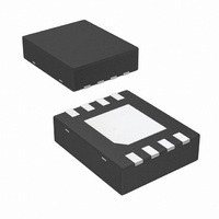
Connection Diagrams 9 Bump micro SMD Package Top View Order Number LM4941TM See NS Package Number TMD09AAA LLP Package Top View Order Number LM4941SD See NS Package Number SDA08C www.national.com micro SMD Markings V = Die Traceability G = Boomer ...
Page 3
... Absolute Maximum Ratings If Military/Aerospace specified devices are required, please contact the National Semiconductor Sales Office/ Distributors for availability and specifications. Supply Voltage Storage Temperature Input Voltage Power Dissipation (Note 3) ESD Susceptibility (Note 4) ESD Susceptibility (Note 5) Junction Temperature Electrical Characteristics V Symbol Parameter ...
Page 4
Electrical Characteristics V Symbol Parameter I Quiescent Power Supply Current DD I Shutdown Current SD P Output Power O THD+N Total Harmonic Distortion + Noise PSRR Power Supply Rejection Ratio CMRR Common-Mode Rejection Ratio V Output Offset Voltage OS V ...
Page 5
Typical Performance Characteristics THD+N vs Output Power = 8Ω 1kHz THD+N vs Frequency = 8Ω 5V 700mW PSRR vs Frequency = 8Ω, Inputs terminated ...
Page 6
CMRR vs Frequency PSRR vs Common Mode Voltage = 8Ω 217Hz Power Dissipation vs Output Power www.national.com = 8Ω 20170373 ...
Page 7
Output Power vs Supply Voltage = 8Ω, Top-THD+N = 10%; Bot-THD Output Power vs Load Resistance Top-V = 5V, 10% THD+N, Topmid-V DD Bot-V = 3V, 10% THD+N, Botmid-V DD Power Derating Curve = 8Ω f ...
Page 8
Application Information OPTIMIZING RF IMMUNITY The internal circuitry of the LM4941 suppresses the amount of RF signal that is coupled into the chip. However, certain external factors, such as output trace length, output trace ori- entation, distance between the chip ...
Page 9
This, however, does not eliminate the need for bypass- ing the supply nodes of the LM4941. The LM4941 will operate without the bypass capacitor C , although the PSRR may de- B crease. A 1µF capacitor is recommended for ...
Page 10
Recommended TM Board Layout Recommended TM Board Layout: Top Layer Recommended TM Board Layout: Bottom Layer www.national.com 20170321 Recommended TM Board Layout: Top Overlay 20170320 10 20170322 ...
Page 11
Recommended LLP Board Layout Recommended LLP Board Layout: Top Layer Recommended LLP Board Layout: Bottom Layer 20170376 Recommended LLP Board Layout: Top Overlay 20170377 11 20170375 www.national.com ...
Page 12
LM4941 Reference Design Boards Bill Of Materials Designator Value Ri1, Ri2 20kΩ Rf1, Rf2 20kΩ 0Ω Ci1, Ci2 1μF Cb, Cs In, Out, VDD, J1 www.national.com Tolerance Part Description 0.10% 1/10W, 0.1% 0805 Resistor 0.10% 1/10W, 0.1% 0805 Resistor 1/10W, ...
Page 13
Revision History Rev Date 1.0 06/28/06 1.1 07/10/06 1.2 08/04/06 1.3 10/12/06 Edited some of the Typical Performance curves' labels and some text edits. 1.4 10/25/06 1.5 11/07/06 1.6 11/15/06 1.7 03/09/07 Changed the Limit value from ...
Page 14
Physical Dimensions www.national.com inches (millimeters) unless otherwise noted micro SMD Package Order Number LM4941TM NS Package Number TMD09AAA X1 = 1.25mm X2 = 1.25mm X3 = 0.6mm LLP Package Order Number LM4941SD NS Package Number SDA08C 14 ...
Page 15
Notes 15 www.national.com ...
Page 16
... National Semiconductor and the National Semiconductor logo are registered trademarks of National Semiconductor Corporation. All other brand or product names may be trademarks or registered trademarks of their respective holders. ...