LM48557TLX/NOPB National Semiconductor, LM48557TLX/NOPB Datasheet
LM48557TLX/NOPB
Specifications of LM48557TLX/NOPB


Related parts for LM48557TLX/NOPB


LM48557TLX/NOPB Summary of contents
Page 1
... The LM48557’s superior click and pop suppression elimi- nates audible transients on power-up/down and during shut- down. The LM48557 is available in an ultra-small 16-bump micro SMD package (1.965mmx1.965mm). Boomer® registered trademark of National Semiconductor Corporation. © 2010 National Semiconductor Corporation LM48557 Key Specifications ■ ...
Page 2
Typical Application www.national.com FIGURE 1. Typical Audio Amplifier Application Circuit 2 30098103 ...
Page 3
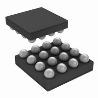
Connection Diagrams TL Package 1.965mm x 1.965mm x 0.6mm Top View Order Number LM48557TL See NS Package Number TLA1611A Ordering Information Order Number Package LM48557TL 16–Bump micro SMD LM48557TLX 16–Bump micro SMD 16–Bump micro SMD Marking 30098112 Package DWG # ...
Page 4
UR Package 1.965mm x 1.965mm x 0.35mm Top View Order Number LM48557UR See NS Package Number URA1611A Ordering Information Order Number Package LM48557UR 16–Bump micro SMD LM48557URX 16–Bump micro SMD www.national.com 16–Bump micro SMD Marking 30098112 Package DWG # Transport ...
Page 5
Bump Descriptions Bump Name SGND A3 VCM A4 B1 OUT- B2 OUT+ B3 RESET B4 C1 CPV C2 C3 SDA C1N D2 PGND Signal Power Supply DD Signal Ground Common ...
Page 6
... Absolute Maximum Ratings 2) If Military/Aerospace specified devices are required, please contact the National Semiconductor Sales Office/ Distributors for availability and specifications. Supply Voltage (Note 1) Storage Temperature Input Voltage Power Dissipation (Note 3) ESD Rating-Human Body Model (Note 4) ESD Rating-Machine Model (Note 5) Junction Temperature ...
Page 7
Symbol Parameter Power Supply Rejection Ratio PSRR (Figure 2) Common Mode Rejection Ratio CMRR (Figure 3) Charge Pump Switching f SW Frequency SNR Signal To Noise Ratio ∈ Output Noise OS T Wake Up Time Interface ...
Page 8
Note 1: “Absolute Maximum Ratings” indicate limits beyond which damage to the device may occur, including inoperability and degradation of device reliability and/or performance. Functional operation of the device and/or non-degradation at the Absolute Maximum Ratings or other conditions beyond ...
Page 9
Typical Performance Characteristics THD+N vs Frequency V = 3.6V 1µF + 22Ω 48dB 2. THD+N vs Output Voltage Z = 1µF + 22Ω Power Consumption vs Output ...
Page 10
CMRR vs Frequency V = 4.2V 200mV DD RIPPLE Output Voltage vs Supply Voltage Z = 1µF + 22Ω, THD Charge Pump Output Voltage vs Load Current V = 4.2V DD www.national.com , A = ...
Page 11
Application Information COMPATIBLE INTERFACE The LM48557 is controlled through an I interface that consists of a serial data line (SDA) and a serial clock (SCL). The clock line is uni-directional. The data line is bi-directional (open drain). ...
Page 12
B7 Device 1 Address Register B7 Name Mode 0 Control Volume 1 Control BIT NAME B0 SHDN B1 MUTE B2 RESERVED* B3 RESERVED* B4 TESTMODE B5 RESERVED* B6 RESERVED* REGISTER B7 ADDRESS *RESERVED bits are Don't Cares and are ignored ...
Page 13
SINGLE AND MULTI-BYTE WRITE OPERATION The LM48557 supports both single-byte and multi-byte write operations. A single-byte write operation begins with the mas- ter device transmitting a START condition followed by the device address (Figure 7). After receiving the correct device ...
Page 14
VOLUME VOL5 STEP 1 0 (MUTE ...
Page 15
VOLUME VOL5 VOL4 STEP ...
Page 16
VOLUME CONTROL The LM48557 has a 64 step volume control, but only 36 steps are recommended for use. Use steps 1 through 32 and steps 61 through 64 to set the gain of the device. Accessing steps 33 through 60 ...
Page 17
SINGLE-ENDED INPUT CONFIGURATION Ground-Referenced Audio Source The LM48557 input stage is compatible with ground-refer- enced input sources, such as CODECs with an integrated headphone amplifier. Connect either input, IN+ or IN- to the FIGURE 9. Single-Ended Input Configuration with a ...
Page 18
PCB Layout Guidelines Minimize trace impedance of the power, ground and all output traces for optimum performance. Voltage loss due to trace resistance between the LM48557 and the load results in de- creased output power and efficiency. Trace resistance be- ...
Page 19
PC Board Layout Silk Screen Layer 2 30098125 Top Layer 30098122 19 30098124 30098123 Layer 3 www.national.com ...
Page 20
Bottom Layer www.national.com 30098120 Bottom Silkscreen 20 30098121 ...
Page 21
Demo Board Schematic FIGURE 11. LM48557 Demo Board Schematic 21 30098119 www.national.com ...
Page 22
Revision History Rev Date 1.0 07/08/09 1.01 07/15/09 1.02 08/05/09 1.03 08/06/09 1.04 01/11/10 www.national.com Description Initial released. Deleted the “Tru-GND...” trademark on the cover page. Text edits. Fixed a typo error. Added the LM48557UR package drawing, top markings, and ...
Page 23
Physical Dimensions inches (millimeters) unless otherwise noted X 16-Bump micro SMD Order Number LM48557TL NS Package Number TLA1611A = 1.965± 0. 1.965 ± 0. 0.6 ± 0.075 www.national.com ...
Page 24
Package Preview 16–Bump micro SMD NS Package Number URA16XXX X = 1.965 ± 0. 1.965 ± 0. 0.350 ± 0.045 ...
Page 25
Notes 25 www.national.com ...
Page 26
... For more National Semiconductor product information and proven design tools, visit the following Web sites at: www.national.com Products Amplifiers www.national.com/amplifiers Audio www.national.com/audio Clock and Timing www.national.com/timing Data Converters www.national.com/adc Interface www.national.com/interface LVDS www.national.com/lvds Power Management www.national.com/power Switching Regulators www.national.com/switchers LDOs www.national.com/ldo LED Lighting www ...