LM49120TLX/NOPB National Semiconductor, LM49120TLX/NOPB Datasheet
LM49120TLX/NOPB
Specifications of LM49120TLX/NOPB


Related parts for LM49120TLX/NOPB


LM49120TLX/NOPB Summary of contents
Page 1
... DD Speaker: ≤ = 8Ω, BTL, THD ■ Output power 3.3V: DD Boomer® registered trademark of National Semiconductor Corporation. © 2008 National Semiconductor Corporation Speaker: = 8Ω, BTL, THD Headphone: = 32Ω, OCL/SE, THD Features ■ ...
Page 2
Typical Application Note:The 6dB speaker gain applies only to the differential input path. www.national.com FIGURE 1. Output Capacitor-less Configuration FIGURE 2. Single-Ended Configuration 2 300375g1 300375n4 ...
Page 3
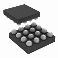
Connection Diagrams 16 Bump micro SMD Package Top View (Bump-Side Down) See NS Package Number TLA1611A Order Number Package LM49120TL 16 Bump micro SMD LM49120TLX 16 Bump micro SMD 300375n2 Ordering Information Package DWG # Transport Media TLA1611A 250 units ...
Page 4
Pin Descriptions Bump www.national.com Name V Headphone Center Amplifier Output OC V Headphone Power Supply DD R Right Channel Headphone Output OUT L Left ...
Page 5
... Absolute Maximum Ratings If Military/Aerospace specified devices are required, please contact the National Semiconductor Sales Office/ Distributors for availability and specifications. Supply Voltage (Note 1) Storage Temperature Input Voltage Power Dissipation (Note 3) ESD Rating (Note 4) ESD Rating (Note 5) Junction Temperature Electrical Characteristics 3.3V ...
Page 6
Symbol Parameter e Output Noise OUT PSRR Power Supply Rejection Ratio VOL Volume Control Step Size Error VOL Digital Volume Control Range RANGE A HP (SE) Mute Attenuation u(HP) MONO_IN Input Impedance and R Input Impedance IN ...
Page 7
Symbol Parameter X Crosstalk TALK T Wake-Up Time from Shutdown WU Electrical Characteristics 5.0V The following specifications apply for V Symbol Parameter I Supply Current DD I Shutdown Current SD V Output Offset Voltage OS P Output Power O THD+N ...
Page 8
Symbol Parameter e Output Noise OUT PSRR Power Supply Rejection Ratio VOL Volume Control Step Size Error VOL Digital Volume Control Range RANGE A HP (SE) Mute Attenuation u(HP) MONO_IN Input Impedance and R Input Impedance IN ...
Page 9
Symbol Parameter X Crosstalk TALK T Wake-Up Time from Shutdown WU Conditions Headphone 12mW OUT f = 1kHz, OCL, Mode 8 Headphone 12mW OUT f = 1kHz, SE, Mode 8 = 4.7μF, OCL ...
Page 10
Timing Characteristics 2.2V The following specifications apply for V Symbol Parameter Clock Period Data Setup Time Data Stable Time Start Condition ...
Page 11
Typical Performance Characteristics Filter BW = 22kHz Crosstalk vs Frequency = 32Ω 3.3V 1kHz, Mode 8, OCL Crosstalk vs Frequency = 32Ω 5V ...
Page 12
Power Dissipation vs Output Power V = 3.3V 1kHz, Mode 8, OCL Power Dissipation vs Output Power 1kHz, Mode 8, OCL Supply Current vs Supply Voltage V ...
Page 13
THD+N vs Frequency = 32Ω 3.3V 12mW 22kHz, Mode 8, SE 30037513 THD+N vs Frequency = 8Ω 3.3V 250mW 1kHz, ...
Page 14
THD+N vs Frequency = 8Ω 5V 1kHz, Mode 1, Speaker THD+N vs Output Power V = 3.3V 1kHz, Mode 8, SE THD+N vs Output Power V = ...
Page 15
THD+N vs Output Power = 32Ω 5V 1kHz, Mode 8, SE 30037525 THD+N vs Output Power = 8Ω 5V 1kHz, Mode 1, Speaker 30037527 PSRR vs ...
Page 16
PSRR vs Frequency = 32Ω 3.3V 200mV , MODE 8, SE RIPPLE P-P PSRR vs Frequency = 32Ω 3.3V 200mV , MODE 4, BTL ...
Page 17
PSRR vs Frequency = 32Ω 2.2μ 5V BYP V = 200mV , MODE 8, OCL RIPPLE P-P 30037540 PSRR vs Frequency = 64Ω 4.7μ 5V BYP ...
Page 18
Application Information COMPATIBLE INTERFACE The LM49120 is controlled through an I interface that consists of a serial data line (SDA) and a serial clock (SCL). The clock line is uni-directional. The data line is bi-directional (open drain). ...
Page 19
B7 B6 Device 1 1 Address B7 B6 Shutdown Control 0 0 Output Mode Control 0 1 Output Gain Control 1 0 Mono Input Volume 1 0 Control Left Input Volume 1 1 Control Right Input Volume 1 1 Control ...
Page 20
Output Mode MC3 MC2 Number ...
Page 21
TABLE 5. Output Mode Control (HP/BTL = 1) Output Mode MC3 MC2 MC1 Number ...
Page 22
Volume Step _G4 ...
Page 23
Bit LS_GAIN BRIDGE CONFIGURATION EXPLAINED The LM49120 loudspeaker amplifier is designed to drive a load differentially, a configuration commonly referred bridge-tied load (BTL). The BTL configuration differs from the single-ended configuration, where one side of the load ...
Page 24
POWER DISSIPATION Power dissipation is a major concern when designing a suc- cessful single-ended or bridged amplifier. A direct consequence of the increased power delivered to the load by a bridge amplifier is higher internal power dissipation. The LM49120 has ...
Page 25
PCB LAYOUT GUIDELINES Minimize trace impedance of the power, ground and all output traces for optimum performance. Voltage loss due to trace resistance between the LM49120 and the load results in de- creased output power and efficiency. Trace resistance be- ...
Page 26
Physical Dimensions X www.national.com inches (millimeters) unless otherwise noted 16 – Bump micro SMD Package Order Number LM49120TL NS Package Number TLA00016 = 2000μm±30m 2000μm±30μ 600μ ...
Page 27
Notes 27 www.national.com ...
Page 28
... For more National Semiconductor product information and proven design tools, visit the following Web sites at: Products Amplifiers www.national.com/amplifiers Audio www.national.com/audio Clock Conditioners www.national.com/timing Data Converters www.national.com/adc Displays www.national.com/displays Ethernet www.national.com/ethernet Interface www.national.com/interface LVDS www.national.com/lvds Power Management www.national.com/power Switching Regulators www.national.com/switchers LDOs www ...