LM49150TLX/NOPB National Semiconductor, LM49150TLX/NOPB Datasheet
LM49150TLX/NOPB
Specifications of LM49150TLX/NOPB


Related parts for LM49150TLX/NOPB


LM49150TLX/NOPB Summary of contents
Page 1
... The LM49150’s superior click and pop suppression elimi- nates audible transients on power-up/down and during shut- down. The LM49150 is available in a ultra-small 20-bump micro SMD package (2.225mm X 2.644mm). Boomer® registered trademark of National Semiconductor Corporation. © 2009 National Semiconductor Corporation LM49150 Key Specifications ■ ...
Page 2
Typical Application FIGURE 1. Typical Audio Amplifier Application Circuit-Output Capacitor-less www.national.com 2 300446n9 ...
Page 3
Connection Diagrams 20 Bump micro SMD Package Top View (Bump Side Down) (See NS Package Number TLA20KGA) Order Number Package LM49150TL 20 Bump micro SMD LM49150TLX 20 Bump micro SMD Top Markings XY - Date Code TT - Die Traceability ...
Page 4
Bump Descriptions Bump Name GND A3 LSOUT- A4 LSOUT SDA B3 SCL B4 LSV C1 INL C2 INR C3 BYPASS C4 CPV D1 INM O(LDO) D3 CPN D4 CPP E1 ...
Page 5
... Absolute Maximum Ratings If Military/Aerospace specified devices are required, please contact the National Semiconductor Sales Office/ Distributors for availability and specifications. Supply Voltage (Note 1) Storage Temperature Input Voltage Power Dissipation (Note 3) ESD Rating (Note 4) ESD Rating (Note 5) Junction Temperature Electrical Characteristics 3.3V The following specifications apply for V = 8Ω ...
Page 6
Symbol Parameter ∈ Output Noise OUT PSRR Power Supply Rejection Ratio Volume Control Step Size Error Digital Volume Control Range A Mute Attenuation M Mono Channel Input Impedance L and R Input Impedance Bypass Resistance ...
Page 7
Electrical Characteristics 5.0V The following specifications apply for V = 8Ω 1kHz, unless otherwise specified. Limits apply for T Symbol Parameter I Supply Current DD I Shutdown Current SD V Output Offset Voltage OS P Output Power O ...
Page 8
Symbol Parameter PSRR Power Supply Rejection Ratio Volume Control Step Size Error Digital Volume Control Range A Mute Attenuation M Mono Channel Input Impedance L and R Input Impedance Bypass Resistance CMRR Common-Mode Rejection Ratio ...
Page 9
micro (Note 2) The following specifications apply for V Symbol Parameter Clock Period Data Setup Time Data Stable Time 3 t Start Condition ...
Page 10
Typical Performance Characteristics THD+N vs Frequency = 8Ω 3.3V Speaker Mode 1 THD+N vs Frequency = 8Ω 5V Speaker Mode 1 THD+N vs Frequency = 8Ω ...
Page 11
THD+N vs Frequency = 8Ω 3.3V 20mW DD L OUT Earpiece Bypass Mode 300446o4 THD+N vs Frequency = 8Ω 5V 60mW DD L OUT Earpiece Bypass Mode 300446o6 THD+N vs ...
Page 12
THD+N vs Output Power = 32Ω 1kHz Headphone Mode 8 CMRR vs Frequency V = 3.3V Loudspeaker Mode 1 CMRR vs Frequency V = 3.3V ...
Page 13
PSRR vs Frequency = 8Ω 3.3V 200mV R DD RIPPLE P-P L Loudspeaker Mode 1 300446t0 PSRR vs Frequency = 32Ω 3.3V 200V R DD RIPPLE P-P L Headphone Mode 4 300446r3 ...
Page 14
Efficiency vs Output Power = 8Ω 1kHz V = 3.6V Speaker Mode 1 Power Dissipation vs Output Power = 8Ω 1kHz R L Speaker Mode 1 Power Dissipation vs Output Power = 8Ω, ...
Page 15
Output Power vs Supply Voltage = 32Ω 1kHz R L Headphone Mode 8 300446q6 Supply Current vs Supply Voltage Headphone Mode 1, No Load 300446q8 Output Power vs Supply Voltage = 8Ω 1kHz R L Earpiece ...
Page 16
Application Information COMPATIBLE INTERFACE The LM49150 is controlled through an I interface that consists of a serial data line (SDA) and a serial clock (SCL). The clock line is uni-directional. The data line is bi-directional (open drain). ...
Page 17
B7 B6 Chip 1 1 Address B7 B6 Shutdown Control 0 0 Spread Spectrum Output Mode Control 0 1 Bypass Output Gain Control 1 0 Mono Input Volume 1 0 Control Left Input Volume 1 1 Control Right Input Volume ...
Page 18
Output Mode MC3 MC2 Number ...
Page 19
TABLE 6. Output Gain Control (Loudspeaker) Bit LS_GAIN TABLE 7. Headphone Output Gain Setting HP_Gain2 HP_Gain1 Value Gain (dB HP_Gain0 0 1 ...
Page 20
Volume Step (1) xG4 ...
Page 21
SINGLE-ENDED INPUT CONFIGURATION The left and right stereo inputs of the LM49150 are configured for single-ended sources (see Figure 1). INPUT CAPACITOR SELECTION Input capacitors may be required for some applications, or when the audio source is single-ended. Input capacitors ...
Page 22
LM49150 Demoboard Bill Of Materials Location Qty CIN2, CIN1 2 0.22uF, 1206, 10V, X7R Ceramic Capacitor CS4, CS2 2 0.1uF, 0805, 10V, X7R Ceramic Capacitor CS7 1 1.0uF, 0805, 10V, X7R Ceramic Capacitor CIN3, CIN4 2 1.0uF 1206, 10V, X7R ...
Page 23
Demo Board Schematic 23 www.national.com ...
Page 24
PC Board Layout Top Silkscreen Layer Layer 2 www.national.com 300446s8 300446s5 24 300446s7 Top Layer 300446s6 Layer 3 ...
Page 25
Bottom Layer 25 300446s4 Bottom Silkscreen www.national.com ...
Page 26
Revision History Rev 1.0 08/27/08 1.01 09/09/08 1.02 03/04/09 www.national.com Date Initial release. Edited Table 6. Added the Layout Guidelines section. 26 Description ...
Page 27
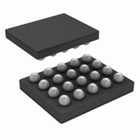
Physical Dimensions inches (millimeters) unless otherwise noted 20 – Bump micro SMD Package Order Number LM49150TL NS Package Number TLA20KGA = 2225μ 2644μm, = 600μ www.national.com ...
Page 28
... For more National Semiconductor product information and proven design tools, visit the following Web sites at: Products Amplifiers www.national.com/amplifiers Audio www.national.com/audio Clock and Timing www.national.com/timing Data Converters www.national.com/adc Interface www.national.com/interface LVDS www.national.com/lvds Power Management www.national.com/power Switching Regulators www.national.com/switchers LDOs www.national.com/ldo LED Lighting www ...