LM4930ITLX/NOPB National Semiconductor, LM4930ITLX/NOPB Datasheet
LM4930ITLX/NOPB
Specifications of LM4930ITLX/NOPB


Related parts for LM4930ITLX/NOPB


LM4930ITLX/NOPB Summary of contents
Page 1
... It is, therefore, ideally suited for mobile phone and other low voltage appli- cations where minimal power consumption is a primary re- quirement. Boomer ® registered trademark of National Semiconductor Corporation. © 2004 National Semiconductor Corporation Key Specifications OUT 1% THD+N ...
Page 2
Typical Application FIGURE 1. Typical I www.national.com Voice codec application circuit for mobile phones 2 20072003 ...
Page 3
Connection Diagrams 36-Bump micro SMD Top View Order Number LM4930ITL See NS Package Number MKT - TLA36KRA 44 – Lead LLP Top View Order Number LM4930LQ See NS Package Number MKT - LQA44A 20072002 20072086 3 micro SMD Marking 20072056 ...
Page 4
Pin Descriptions A1 MIC_P A2 MIC_N A3 AVDD_MIC A4 DAC_REF A5 SDA A6 SCL B1 AGND_MIC B2 MIC_BIAS B3 MIC_REF B4 ADDR B5 PCM_SDI B6 PCM_CLK C1 AVDD_HP BYPASS C4 PCM_SYNC C5 I2S_DATA C6 DGND_D D1 HP_L ...
Page 5
System Control Registers The LM4930 is controlled with a two-wire serial interface. This interface is used to configure the operating mode, digi- tal interfaces, and delta-sigma modulators. The LM4930 is This register is used to configure the I BASICCONFIG register ...
Page 6
System Control Registers This register configures the voiceband codec, sidetone attenuation, and selected control functions. The 7 bit address for the VOICE TESTCONFIG register is XX10001. VOICETESTCONFIG (XX10001). (Set = logic 1, Clear = logic 0) BIT ...
Page 7
System Control Registers This register is used to control the gain of the headphone amplifier, the loudspeaker amplifier, and the microphone preampli- fier. The 7 bit address for the GAINCONFIG register is XX10010. to logic 1) GAINCONFIG (XX10010). (Set = ...
Page 8
System Control Registers 13:10 0000 0001 0010 0011 0100 0101 0110 0111 1000 1001 1010 1011 1100 1101 1110 1111 15:14 RSVD RESERVED (Note 13) www.national.com (Continued) GAIN CONFIG REGISTERS (Continued) Mic Preamp Gain 17dB 19dB 21dB 23dB 25dB 27dB ...
Page 9
Timing Diagrams FIGURE 2. Two-wire control Interface Timing Diagram FIGURE 3. PCM Receive Timing Diagram 2 FIGURE Transmit Timing Diagram 9 20072009 20072008 20072007 www.national.com ...
Page 10
... Absolute Maximum Ratings If Military/Aerospace specified devices are required, please contact the National Semiconductor Sales Office/ Distributors for availability and specifications. Analog Supply Voltage Digital Storage Supply Voltage Storage temperature Power Dissipation (Note 3) ESD Susceptibility Human Body Model (Note 4) Machine Model (Note 5) ...
Page 11
Electrical Characteristics DV (Notes (Continued) The following specifications apply for the circuit shown in Figure 1, unless otherwise specified. Limits apply for T Symbol Parameter V Mic Bias Voltage MIC_BIAS THD+N Headphone Amplifier Total Harmonic Motion Distortion ...
Page 12
Electrical Characteristics DV (Notes (Continued) The following specifications apply for the circuit shown in Figure 1, unless otherwise specified. Limits apply for T Symbol Parameter LPB Voice ADC Lower Passband VADC Cutoff Frequency. SBA Voice ADC Stopband ...
Page 13
Electrical Characteristics DV (Notes (Continued) The following specifications apply for the circuit shown in Figure 1, unless otherwise specified. Limits apply for T Symbol Parameter f PCM_CLK Frequency CLKPCM PCM_CLK Duty Cycle f I2S_CLK Frequency CLKI2S I2S_CLK ...
Page 14
Electrical Characteristics DV (Notes (Continued) The following specifications apply for the circuit shown in Figure 1, unless otherwise specified. Limits apply for T Symbol Parameter AI Analog Standby Current ST V Full-Scale Output Voltage FS_LS (Mono speaker ...
Page 15
Electrical Characteristics DV (Notes (Continued) The following specifications apply for the circuit shown in Figure 1, unless otherwise specified. Limits apply for T Symbol Parameter SBA Voice DAC Stopband Attenuation VDAC UPB Voice ADC Upper Passband VADC ...
Page 16
Electrical Characteristics DV (Notes (Continued) The following specifications apply for the circuit shown in Figure 1, unless otherwise specified. Limits apply for T Symbol Parameter t SDA_DATA Setup Time SDAS f PCM_CLK Frequency CLKPCM PCM_CLK Duty Cycle ...
Page 17
Typical Performance Characteristics MIC PreAmp + ADC Frequency Response (MIC Gain = 17dB) MIC PreAmp + ADC Frequency Response (MIC Gain = 47dB) MIC PreAmp + ADC Frequency Response High Cutoff (MIC Gain = 17dB) (Note 16) MIC PreAmp + ...
Page 18
Typical Performance Characteristics MIC PreAmp + ADC Frequency Response Low Cutoff (MIC Gain = 17dB) ADC THD+N vs MIC Input Voltage (MIC Gain = 17dB) MIC PreAmp + ADC PSRR vs Frequency Top Trace = 47dB MIC Gain, Bottom Trace ...
Page 19
Typical Performance Characteristics Headphone Sense In Hysteresis Loop ( DAC Frequency Response Zoom (Handsfree Output DAC Frequency Response Zoom (Headphone Output) (Note 16) (Continued DAC Frequency Response ( ...
Page 20
Typical Performance Characteristics 2 THD Input Voltage (Headphone Output, 0dB Headphone Gain) MIC Bias Dropout Voltage vs MIC Bias Current PCM DAC Frequency Response Zoom (Handsfree Output) www.national.com (Note 16) (Continued (Top Trace = Left ...
Page 21
Typical Performance Characteristics PCM DAC Frequency Response Zoom (Headphone Output) THD+N vs PCM Input Voltage (Headphone Output, 0dB Headphone Gain) PSRR vs Frequency ( 16Ω, Headphone Output (Note 16) (Continued) THD+N vs PCM Input ...
Page 22
Typical Performance Characteristics PSRR vs Frequency ( 8Ω, Handsfree Output PSRR vs Frequency ( 32Ω, Headphone Output THD+N vs Frequency ( 8Ω ...
Page 23
Typical Performance Characteristics THD+N vs Frequency ( and 32Ω Headphone Output) THD+N vs Output Power 16Ω 1kHz, Headphone Output THD+N ...
Page 24
Typical Performance Characteristics Application Information REFERENCE DESIGN BOARD AND LAYOUT LM4930ITL Board Layout www.national.com (Note 16) (Continued) THD+N vs Output Power ( 8Ω 1kHz, Handsfree Output FIGURE 5. LM4930ITL Demo Board Schematic ...
Page 25
Application Information FIGURE 6. LM4930ITL Demo Board Composite View (Continued) FIGURE 7. LM4930ITL Demo Board Silkscreen 25 20072006 20072005 www.national.com ...
Page 26
Application Information www.national.com (Continued) FIGURE 8. LM4930ITL Demo Board Top Layer FIGURE 9. LM4930ITL Demo Board Bottom Layer 26 20072004 20072013 ...
Page 27
Application Information FIGURE 10. LM4930ITL Demo Board Inner Layer 1 FIGURE 11. LM4930ITL Demo Board Inner Layer 2 (Continued) 27 20072012 20072011 www.national.com ...
Page 28
Application Information FIGURE 12. Pin Markings for LM4930ITL demo board BILL OF MATERIALS FOR LM4930 LM4930 Demo Board Bill Of Materials Comment 1k 2k 20k 100k 1M 22pF 0.01µF cer 0.1µF cer 1µF 220µF CRYSTAL PHONE JACK STEREO SW STEREO ...
Page 29
Application Information Pin Header Pin Pin Pin 1 2 Pin 1 2 Pin (Continued) Two-wire control Interface ...
Page 30
Application Information 1 2 ADR SELECT (S1) Jumper IN = LOW Control interface responds to addresses 001000b (BASICCONFIG), 0010001b (VOICETESTCONFIG)), and 0010010b (GAIN- CONFIG) Jumper OUT = HIGH Control interface responds to addresses 111000b (BASICCONFIG), 1110001b (VOICETESTCONFIG)), and 1110010b (GAIN- ...
Page 31
Application Information patible with the interface header (J1) on the LM4930 board. This also features demonstration software to allow for com- plete control and evaluation of the various modes and func- tions of the LM4930 through the bus. Pullup resistors ...
Page 32
Application Information MIC Jack (J3) This jack is for connection to an external microphone like the kind typically found in mobile phones. Pin 1 is GND, pin 2 is the negative input pin, and pin 3 is the positive pin, ...
Page 33
Application Information A single-ended stereo headphone output is also featured, providing up to 30mW of power per channel into 32Ω with a 5V analog supply. A Headphone Sense output is provided on J6 for connection to an external controller. This ...
Page 34
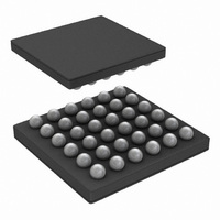
Physical Dimensions X www.national.com inches (millimeters) unless otherwise noted 36-Bump micro SMD Order Number LM4930ITL NS Package Number TLA36KRA ± ± = 3.230 0.03mm X = 3.408 0. ± = 0.600 0.075 ...
Page 35
... BANNED SUBSTANCE COMPLIANCE National Semiconductor certifies that the products and packing materials meet the provisions of the Customer Products Stewardship Specification (CSP-9-111C2) and the Banned Substances and Materials of Interest Specification (CSP-9-111S2) and contain no ‘‘Banned Substances’’ as defined in CSP-9-111S2. ...