MAX4060ETA+T Maxim Integrated Products, MAX4060ETA+T Datasheet - Page 2
MAX4060ETA+T
Manufacturer Part Number
MAX4060ETA+T
Description
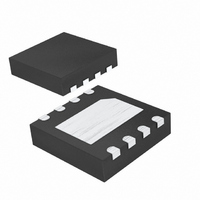
IC PREAMP AUDIO STER AB 8TDFN
Manufacturer
Maxim Integrated Products
Type
Class ABr
Datasheet
1.MAX4061ETAT.pdf
(17 pages)
Specifications of MAX4060ETA+T
Output Type
2-Channel (Stereo)
Voltage - Supply
4.5 V ~ 5.5 V
Features
Differential Inputs, Microphone
Mounting Type
Surface Mount
Package / Case
8-TDFN Exposed Pad
Lead Free Status / RoHS Status
Lead free / RoHS Compliant
Max Output Power X Channels @ Load
-


ABSOLUTE MAXIMUM RATINGS
Supply Voltage (V
Any Other Pin to GND ................................-0.3V to (V
Duration of Short Circuit to GND or V
Continuous Input Current (any pin) ................................ ±10mA
Continuous Power Dissipation (T
Differential Microphone Preamplifiers with
Internal Bias and Complete Shutdown
Stresses beyond those listed under “Absolute Maximum Ratings” may cause permanent damage to the device. These are stress ratings only, and functional
operation of the device at these or any other conditions beyond those indicated in the operational sections of the specifications is not implied. Exposure to
absolute maximum rating conditions for extended periods may affect device reliability.
ELECTRICAL CHARACTERISTICS
(V
R
2
Supply Voltage Range
Supply Current
Output Common-Mode Voltage
Slew Rate
Supply Current in Shutdown
Output Short-Circuit Current
DIFFERENTIAL INPUT (INT/AUX = 0V for MAX4060/MAX4062, default for MAX4061)
Input Offset Voltage
Common-Mode Input Voltage
Range
Maximum Differential Input
Voltage
Small-Signal Bandwidth
Input Resistance
Input Resistance Match
Input Noise-Voltage Density
RMS Output Noise Voltage
L
CC
8-Pin Thin QFN (derate 4.7mW/°C above +70°C) ......379mW
8-Pin µMAX (derate 4.1mW/°C above +70°C) ............330mW
= 100k to 1.5V, R
_______________________________________________________________________________________
= 3V for MAX4061/MAX4062, V
PARAMETER
CC
to GND). .................................-0.3V to +6V
BIAS
= , T
A
A
= +70°C)
= T
CC
SYMBOL
V
MIN
R
BW
DIFFMAX
V
....................Continuous
I
V
MATCH
SHDN
V
V
V
NRMS
I
OCM
I
R
SR
CC
SC
e
CC
CM
OS
CC
-3dB
IN
to T
n
= 5V for MAX4060, GND = 0V,
MAX
Inferred from
PSRR test
A
V
To GND
To V
A
Either differential input
A
A
only
A
, unless otherwise noted. Typical values are at T
V
V
V
V
V
SHDN
CC
= 10V/V
= 1V/V, MAX4061/MAX4062
= 10V/V, f = 1kHz
= 100V/V, f = 1kHz, MAX4061/MAX4062
= 10V/V, BW = 22Hz to 22kHz
CC
+ 0.3V)
= 0V, MAX4061
CONDITIONS
Operating Temperature Range ...........................-40°C to +85°C
Junction Temperature ......................................................+150°C
Storage Temperature Range .............................-65°C to +150°C
Lead Temperature (soldering, 10s) .................................+300°C
10-Pin µMAX (derate 5.6mW/°C above +70°C) .........444mW
MAX4061/MAX4062
MAX4060
SHDN = V
CC
, INT/AUX = 0V, R
A
1.25
MIN
2.4
4.5
= +25°C.) (Notes 1, 2)
1
0.001
TYP
0.75
600
100
100
125
1.5
30
30
20
0.1
1
1
1
MAX
1.75
5.5
5.5
1.2
1
2
G
5
= 11.11k ,
nV/ Hz
UNITS
µV
V/µs
kHz
mA
mA
mV
k
µA
%
V
V
V
V
RMS
Related parts for MAX4060ETA+T
Image
Part Number
Description
Manufacturer
Datasheet
Request
R

Part Number:
Description:
HIGH CURRENT TRANSIENT VOLTAGE SUPPRESSOR (TVS) DIODE
Manufacturer:
MDE [MDE Semiconductor, Inc.]
Datasheet:
Part Number:
Description:
HIGH CURRENT TRANSIENT VOLTAGE SUPPRESSOR (TVS) DIODE STAND-OFF VOLTAGE 12 TO 150 Volts 40000 Watt Peak Pulse Power
Manufacturer:
MDE [MDE Semiconductor, Inc.]
Datasheet:

Part Number:
Description:
MAX7528KCWPMaxim Integrated Products [CMOS Dual 8-Bit Buffered Multiplying DACs]
Manufacturer:
Maxim Integrated Products
Datasheet:
Part Number:
Description:
Single +5V, fully integrated, 1.25Gbps laser diode driver.
Manufacturer:
Maxim Integrated Products
Datasheet:
Part Number:
Description:
Single +5V, fully integrated, 155Mbps laser diode driver.
Manufacturer:
Maxim Integrated Products
Datasheet:
Part Number:
Description:
VRD11/VRD10, K8 Rev F 2/3/4-Phase PWM Controllers with Integrated Dual MOSFET Drivers
Manufacturer:
Maxim Integrated Products
Datasheet:
Part Number:
Description:
Highly Integrated Level 2 SMBus Battery Chargers
Manufacturer:
Maxim Integrated Products
Datasheet:
Part Number:
Description:
Current Monitor and Accumulator with Integrated Sense Resistor; ; Temperature Range: -40°C to +85°C
Manufacturer:
Maxim Integrated Products
Part Number:
Description:
TSSOP 14/A°/RS-485 Transceivers with Integrated 100O/120O Termination Resis
Manufacturer:
Maxim Integrated Products
Part Number:
Description:
TSSOP 14/A°/RS-485 Transceivers with Integrated 100O/120O Termination Resis
Manufacturer:
Maxim Integrated Products
Part Number:
Description:
QFN 16/A°/AC-DC and DC-DC Peak-Current-Mode Converters with Integrated Step
Manufacturer:
Maxim Integrated Products
Part Number:
Description:
TDFN/A/65V, 1A, 600KHZ, SYNCHRONOUS STEP-DOWN REGULATOR WITH INTEGRATED SWI
Manufacturer:
Maxim Integrated Products
Part Number:
Description:
Integrated Temperature Controller f
Manufacturer:
Maxim Integrated Products
Part Number:
Description:
SOT23-6/I°/45MHz to 650MHz, Integrated IF VCOs with Differential Output
Manufacturer:
Maxim Integrated Products
Part Number:
Description:
SOT23-6/I°/45MHz to 650MHz, Integrated IF VCOs with Differential Output
Manufacturer:
Maxim Integrated Products