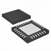
MAX9850ETI+T Maxim Integrated Products, MAX9850ETI+T Datasheet - Page 12

MAX9850ETI+T
Manufacturer Part Number
MAX9850ETI+T
Description
IC AMP AUDIO .095W STER 28TQFN
Manufacturer
Maxim Integrated Products
Series
DirectDrive™r
Type
Class ABr
Datasheet
1.MAX9850ETI.pdf
(36 pages)
Specifications of MAX9850ETI+T
Output Type
Headphones, 2-Channel (Stereo)
Max Output Power X Channels @ Load
95mW x 2 @ 16 Ohm
Voltage - Supply
1.8 V ~ 3.6 V
Features
DAC, Depop, Digital Inputs, I²C, I²S, Line Level Inputs & Outputs, Mute, Shutdown, Volume Control
Mounting Type
Surface Mount
Package / Case
28-WQFN Exposed Pad, 28-HWQFN
Lead Free Status / RoHS Status
Lead free / RoHS Compliant
Stereo Audio DAC with DirectDrive
Headphone Amplifier
12
______________________________________________________________________________________
PIN
10
11
12
13
14
15
16
17
18
19
20
21
22
23
24
25
26
27
28
—
1
2
3
4
5
6
7
8
9
LRCLK
NAME
DGND
AGND
PGND
MCLK
OUTR
NREG
BCLK
DV
OUTL
PREG
GPIO
AV
PV
SDIN
SV
PV
ADD
HPR
C1N
SDA
HPL
HPS
C1P
SCL
INR
REF
INL
EP
DD
DD
DD
SS
SS
Digital Audio Left-Right Clock Input/Output. LRCLK is the audio sample rate clock and determines
whether the audio data on SDIN is routed to the left or right channel. LRCLK is an input when the
MAX9850 is in slave mode and an output when in master mode.
Digital Audio Bit Clock Input/Output. BCLK is an input when the MAX9850 is in slave mode and an
output when in master mode.
Digital Audio Serial Data Input
Digital Power-Supply Input. Bypass to DGND with a 1µF ceramic capacitor.
Master Clock Input. All internal digital clocks are derived from MCLK.
Digital Ground
I
addresses.
General-Purpose Input/Output. Configure GPIO as an input or an output through the GPIO register.
GPIO can perform the function of an interrupt when configured as an output. See the GPIO section.
Right-Channel Line Input. INR is mixed with the right DAC output.
Left-Channel Line Input. INL is mixed with the left DAC output.
Line Level Right-Channel Output. OUTR is biased at AGND.
Line Level Left-Channel Output. OUTL is biased at AGND.
Reference Output. Bypass to AGND with a 1µF ceramic capacitor.
Analog Ground
Line Output Negative Regulator Output. Bypass to AGND with a 1µF capacitor.
Line Output Positive Regulator Output. Bypass to AGND with a 1µF capacitor.
Analog Power Supply. Bypass to AGND with a 1µF ceramic capacitor.
Right-Channel Headphone Output. HPR is a DirectDrive output biased at AGND.
Left-Channel Headphone Output. HPL is a DirectDrive output biased at AGND.
Headphone Amplifier Negative Power-Supply Input. Connect to PV
Headphone Sense Input. Connect to the control pin of a headphone jack for automatic headphone
sensing. Float HPS if unused. See the Headphone Sense Input (HPS) section.
Inverting Charge-Pump Output. Bypass to PGND with a 2.2µF ceramic capacitor and connect to SV
to provide the headphone amplifiers with a negative supply.
Charge-Pump Flying Capacitor Negative Terminal. Connect a 0.47µF ceramic capacitor between
C1N and C1P.
Charge-Pump Ground
Charge-Pump Flying Capacitor Positive Terminal. Connect a 0.47µF ceramic capacitor between C1P
and C1N.
Charge-Pump and Headphone Amplifier Positive Power-Supply Input. Bypass to PGND with a 1µF
ceramic capacitor. Connect to AV
I
I
Exposed Thermal Pad. Connect EP to AGND.
2
2
2
C Address-Select Input. Connect to AGND, AV
C-Compatible Serial Clock Input
C-Compatible Serial Data Input/Output
DD
for normal operation.
FUNCTION
DD
, or SDA to select one of the three possible I
SS
.
Pin Description
2
C
SS


