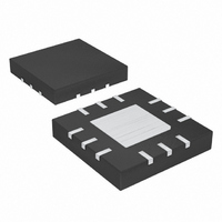
MAX9724BETC+ Maxim Integrated Products, MAX9724BETC+ Datasheet - Page 14

MAX9724BETC+
Manufacturer Part Number
MAX9724BETC+
Description
IC AMP AUDIO .045W STER 12TQFN
Manufacturer
Maxim Integrated Products
Series
DirectDrive™r
Type
Class ABr
Datasheet
1.MAX9724AETC.pdf
(19 pages)
Specifications of MAX9724BETC+
Output Type
Headphones, 2-Channel (Stereo)
Max Output Power X Channels @ Load
63mW x 2 @ 32 Ohm
Voltage - Supply
2.7 V ~ 5.5 V
Features
Depop, Short-Circuit and Thermal Protection, Shutdown
Mounting Type
Surface Mount
Package / Case
12-TQFN Exposed Pad
Product
General Purpose Audio Amplifiers
Output Power
42 mW
Thd Plus Noise
0.02 %
Supply Current
3.5 mA
Maximum Power Dissipation
1333 mW
Maximum Operating Temperature
+ 85 C
Mounting Style
SMD/SMT
Audio Load Resistance
16 Ohms
Minimum Operating Temperature
- 40 C
Amplifier Class
AB
No. Of Channels
2
Supply Voltage Range
2.7V To 5.5V
Load Impedance
16ohm
Operating Temperature Range
-40°C To +85°C
Amplifier Case Style
TQFN
Rohs Compliant
Yes
For Use With
MAX9724AEVKIT+ - EVALUATION KIT FOR MAX9724A/BMAX9724DEVKIT+ - KIT EVAL FOR MAX9724D
Lead Free Status / RoHS Status
Lead free / RoHS Compliant
60mW, DirectDrive, Stereo Headphone Amplifier
with Low RF Susceptibility and Shutdown
To suppress this noise, and to provide a 2V
dard audio output level from a single 5V supply, the
MAX9724A can be configured as a line driver and
active lowpass filter. Figure 5 shows the MAX9724A
connected as 2-pole Rauch/multiple feedback filter with
a passband gain of 6dB and a -3dB (below passband)
cutoff frequency of approximately 27kHz (see Figure 6
for the Gain vs. Frequency plot).
Proper layout and grounding are essential for optimum
performance. Connect PGND and SGND together at a
single point on the PC Board. Connect PV
and bypass with a 1µF capacitor. Place the power-sup-
ply bypass capacitor and the charge-pump hold
capacitor as close to the MAX9724 as possible. Route
PGND and all traces that carry switching transients
away from SGND and the audio signal path. The thin
QFN package features an exposed paddle that
improves thermal efficiency. Ensure that the exposed
paddle is electrically isolated from PGND, SGND,
and V
when the board layout dictates that the exposed
paddle cannot be left floating.
For the latest application details on UCSP construction,
dimensions, tape carrier information, printed circuit
board techniques, bump-pad layout, and recommend-
ed reflow temperature profile, as well as the latest infor-
mation on reliability testing results, refer to the
Application Note UCSP—A Wafer-Level Chip-Scale
Package available on Maxim’s website at www.maxim-
ic.com/ucsp.
14
______________________________________________________________________________________
UCSP Applications Information
DD
. Connect the exposed paddle to SV
Layout and Grounding
SS
RMS
to SV
SS
stan-
only
SS
Figure 6. Frequency Response of Active Filter of Figure 4
-10
-15
-20
-25
-30
-35
10
-5
5
0
1k
MAX9724A ACTIVE FILTER GAIN
vs. FREQUENCY
10k
FREQUENCY (Hz)
100k
R
L
= 10kΩ
1M


