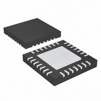
MAX9770ETI+ Maxim Integrated Products, MAX9770ETI+ Datasheet - Page 14

MAX9770ETI+
Manufacturer Part Number
MAX9770ETI+
Description
IC AMP AUDIO 1.2W MONO D 28TQFN
Manufacturer
Maxim Integrated Products
Type
Class Dr
Datasheet
1.MAX9770ETIT.pdf
(22 pages)
Specifications of MAX9770ETI+
Output Type
1-Channel (Mono) with Stereo Headphones
Max Output Power X Channels @ Load
1.2W x 1 @ 8 Ohm; 80mW x 2 @ 16 Ohm
Voltage - Supply
2.5 V ~ 5.5 V
Features
Depop, Input Multiplexer, Mute, Short-Circuit and Thermal Protection, Shutdown
Mounting Type
Surface Mount
Package / Case
28-TQFN Exposed Pad
Lead Free Status / RoHS Status
Lead free / RoHS Compliant
Maxim’s DirectDrive architecture uses a charge pump to
create an internal negative supply voltage. This allows
the headphone outputs of the MAX9770 to be biased
about GND, almost doubling dynamic range while oper-
ating from a single supply. With no DC component, there
is no need for the large DC-blocking capacitors. Instead
of two large (220µF, typ) tantalum capacitors, the
MAX9770 charge pump requires two small ceramic
capacitors, which conserves board space, reduces cost,
and improves the frequency response of the headphone
driver. See the Output Power vs. Charge-Pump
Capacitance and Load Resistance graph in the Typical
Operating Characteristics for details of the possible
capacitor sizes. There is a low DC voltage on the driver
outputs due to amplifier offset. However, the offset of the
MAX9770 is typically 5mV, which, when combined with a
32Ω load, results in less than 160µA of DC current flow
to the headphones.
In addition to the cost and size disadvantages of the DC-
blocking capacitors required by conventional head-
phone amplifiers, these capacitors limit the amplifier’s
low-frequency response and can distort the audio signal.
Previous attempts at eliminating the output-coupling
capacitors involved biasing the headphone return
(sleeve) to the DC bias voltage of the headphone
amplifiers. This method raises some issues:
1) When combining a microphone and headphone on a
1.2W, Low-EMI, Filterless, Mono Class D Amplifier
with Stereo DirectDrive Headphone Amplifiers
Figure 4. MAX9770 Output with No Signal Applied
14
single connector, the microphone bias scheme typi-
cally requires a 0V reference.
V OUT+ - V OUT- = 0V
______________________________________________________________________________________
V IN = 0V
OUT+
OUT-
2) The sleeve is typically grounded to the chassis.
3) During an ESD strike, the driver’s ESD structures are
4) When using the headphone jack as a line out to
Figure 5. MAX9770 Efficiency vs. Class AB Efficiency
Figure 6. HPS Configuration
Using the midrail biasing approach, the sleeve must
be isolated from system ground, complicating prod-
uct design.
the only path to system ground. Thus, the driver
must be able to withstand the full ESD strike.
other equipment, the bias voltage on the sleeve may
conflict with the ground potential from other equip-
ment, resulting in possible damage to the drivers.
SHDN
100
90
80
70
60
50
40
30
20
10
0
SHUTDOWN
CONTROL
0
EFFICIENCY vs. OUTPUT POWER
HPOUTL
HPOUTR
0.1
MAX9770
HPS
MAX9770
10kΩ
OUTPUT POWER (W)
CLASS AB
0.2
800kΩ
10kΩ
0.3
V
DD
0.4
V
f = 1kHz
R
DD
L
- 8Ω
0.5
= 3.3V
0.6


